
Complete PCB Chip Package Soldering Methods and Workflow

At Highleap Electronics, we specialize in PCB manufacturing and assembly, understanding that PCB chip package soldering is a fundamental process in the production of high-quality, reliable electronic devices. As the electronics industry evolves, so does the complexity of soldering methods used to assemble printed circuit boards (PCBs). This comprehensive guide delves into the critical techniques and best practices involved in PCB chip package soldering, focusing on different chip package types, selection criteria, soldering methods, and the importance of precision in ensuring optimal product quality.
Understanding Chip Packages and Their Selection Criteria for PCB Assembly
Choosing the right chip package is one of the first and most important steps in PCB assembly. The type of chip package directly influences the soldering process, board design, and overall performance of the electronic device. For successful PCB chip package soldering, it’s essential to understand the various package types and their selection criteria.
Types of Chip Packages
- DIP (Dual In-line Package): Traditionally used for through-hole mounting, this package type is primarily used in older electronic designs or for prototyping.
- QFP (Quad Flat Package): A popular surface-mount option for microcontrollers and processors, offering a higher pin count and allowing for compact design layouts.
- BGA (Ball Grid Array): Known for high-density interconnections, BGA packages are commonly used in high-performance computing and telecommunications, offering enhanced thermal management and electrical performance.
- SOIC (Small Outline Integrated Circuit): This surface-mount package is often used in general consumer electronics, offering a smaller footprint for moderate-density circuits.
Factors for Package Selection
The choice of chip package depends on several factors, including electrical requirements (signal integrity, power consumption), mechanical constraints (board space, thermal management), and thermal properties. For instance, BGA packages are ideal for high-performance applications, while SOIC packages are preferred when space is limited.
Soldering Methods: Surface Mount vs. Through-Hole Soldering for PCB Assembly
Once the chip package has been selected, the next step is choosing the appropriate soldering technique to ensure a reliable and durable connection between the component and the PCB. Soldering methods vary based on the type of package being used, with different methods offering distinct advantages for different production volumes.
Surface Mount Technology (SMT) and Reflow Soldering
Surface Mount Technology (SMT) is the most common soldering method used in modern PCB assembly due to its efficiency, especially for high-density boards. Reflow soldering is the primary technique for SMT, involving the use of solder paste and heat to create strong connections between components and PCB pads.
Reflow Soldering Process:
-
- Preheat: The PCB and components are heated to a moderate temperature (100°C-150°C) to remove moisture from the components.
- Soak: Flux activation occurs at temperatures of 150°C to 180°C.
- Reflow: The solder paste melts at temperatures between 217°C to 250°C, creating solid bonds between components and the PCB.
- Cooling: The PCB is slowly cooled to solidify the solder.
Through-Hole Soldering for Enhanced Mechanical Strength
Through-hole soldering remains a reliable method for components that require mechanical stability and high-strength connections. This technique is often used for larger components or when the component needs to be securely mounted to withstand mechanical stress. Methods like wave soldering or selective soldering are often used in these applications for high-volume production.
Advanced Soldering Techniques for Complex PCB Packages
As PCBs grow in complexity, especially with high-performance packages like BGA, advanced soldering methods are necessary to ensure precise, reliable connections. These techniques address the unique challenges posed by miniaturization, complex component designs, and sensitive materials.
Specialized Techniques for Soldering BGA Packages
Soldering BGA (Ball Grid Array) packages requires advanced techniques due to the hidden solder joints located beneath the package, making them difficult to inspect and repair using traditional methods. To ensure high-quality connections and prevent defects, several specialized techniques are employed throughout the soldering process.
- X-ray Inspection: X-ray inspection is a critical tool in BGA soldering, as it enables the inspection of solder joints that are otherwise inaccessible. This technique is used to detect hidden defects such as solder bridges, voids, incomplete solder joints, misalignment, or cracks that may affect the electrical conductivity and overall reliability of the PCB. X-ray inspection can also be used to examine the internal structure of the BGA package, including the ball-to-pad connection, ensuring that all solder joints are formed correctly.
- BGA Bubble Detection: During the soldering process, air bubbles may form under the BGA package, especially during the reflow process. These bubbles can lead to weak or unreliable solder joints, affecting the electrical performance and reliability of the PCB. To detect and prevent such issues, advanced X-ray systems are used to scan the BGA package for any trapped air or bubbles. Identifying these bubbles early on allows manufacturers to take corrective actions, ensuring that the final product maintains its quality and functionality.
- Reflow Process Control: A precisely controlled reflow process is essential to ensure uniform heating of the BGA package and proper solder joint formation. Reflow ovens equipped with thermal profiling systems are used to regulate the temperature throughout the soldering process. These systems ensure that the BGA package reaches the optimal temperature for solder melting and solidification, preventing defects such as cold joints, solder bridges, or insufficient solder. Accurate temperature control also reduces the risk of overheating, which could damage sensitive components.
- Miniaturization and Micro-Soldering Techniques: As electronic devices become smaller and more complex, miniaturization presents additional challenges in BGA soldering. Micro-soldering techniques, such as using fine-tipped soldering tools and advanced optical alignment systems, are employed to handle smaller components with extreme precision. These tools allow for better control over the application of solder, ensuring that even the smallest BGA packages are properly soldered without causing damage to nearby components or creating defective joints.
- Flux and Solder Paste Application: The application of flux and solder paste is critical in BGA soldering to ensure proper wetting and to avoid issues like solder bridges or cold joints. Specialized dispensing equipment is used to apply flux and solder paste precisely to the PCB pads before the BGA package is placed. The flux helps remove oxidation from the pads, while the solder paste ensures a strong connection between the BGA balls and the PCB pads during reflow. The correct amount of solder paste must be applied to prevent excess or insufficient solder, which could lead to defects.
- Automated Optical Inspection (AOI): Automated Optical Inspection (AOI) is used in combination with other techniques to inspect the external appearance of BGA solder joints. AOI systems capture high-resolution images of the BGA package and use advanced image processing algorithms to detect surface defects such as misalignment, solder bridges, or insufficient solder. While X-ray inspection focuses on internal defects, AOI ensures that external visual defects are also detected early in the production process.
- Solder Joint Reliability Testing: In addition to visual inspection and X-ray analysis, reliability testing is an essential step in BGA soldering. Methods such as thermal cycling tests and mechanical stress tests are used to simulate real-world conditions and assess the durability of the solder joints. These tests help identify potential failure points and ensure that the BGA solder joints can withstand temperature variations and mechanical stress during the product’s lifecycle.
- BGA Rework and Repair Techniques: In cases where defects are detected after the BGA package has been soldered, rework techniques such as hot-air reflow or laser soldering may be used to correct the solder joints. These methods allow for precise heat application to reflow the solder and correct any misaligned or insufficient joints without causing damage to the surrounding components. Additionally, BGA packages that are defective or misaligned can be carefully removed and replaced using specialized tools, ensuring the integrity of the PCB.
By combining these specialized techniques, such as X-ray inspection, BGA bubble detection, reflow process control, micro-soldering, and reliability testing, manufacturers can ensure the high quality and reliability of BGA solder joints. These methods help prevent defects, ensure consistent soldering performance, and enhance the overall functionality of the final product, making BGA soldering a key aspect of advanced PCB assembly.

Pre-Soldering Preparation: Ensuring Optimal Conditions for Soldering
Before the soldering process begins, careful preparation of both the workspace and components is crucial to avoid defects and ensure high-quality solder joints. This preparation involves several steps, including setting up the proper environment and implementing strict handling protocols for sensitive components.
Optimal Workspace Setup
- Temperature Control: Maintaining a consistent temperature of 20-25°C in the workspace is essential for achieving reliable soldering results.
- ESD Protection: Using grounded wrist straps, anti-static mats, and a static-free environment is vital to prevent electrostatic discharge (ESD) that could damage sensitive components during handling.
- Lighting: Proper lighting ensures that solder joints can be clearly inspected and components placed with accuracy.
Component Handling and Storage
- Moisture Protection: Components must be stored in moisture-barrier packaging to prevent damage from humidity. A controlled storage environment with the right temperature is necessary for preserving component integrity.
Post-Soldering Inspection and Quality Control
After the soldering process is complete, it’s essential to inspect the PCB for defects to ensure the connections are reliable and meet industry standards.
Common Soldering Defects and Prevention
- Solder Bridging: Occurs when excess solder causes unintended connections. This can be prevented by applying solder paste precisely and controlling the reflow process.
- Cold Joints: Result from insufficient heat application during soldering, leading to weak or unreliable connections. Proper temperature control during soldering helps prevent cold joints.
- Tombstoning: When a component lifts off the PCB during soldering due to uneven heating. This can be avoided by ensuring a balanced thermal profile throughout the reflow process.
- BGA Bubble Detection: Ball Grid Array (BGA) soldering can sometimes result in bubbles trapped under the component, leading to potential defects in electrical connections. BGA bubble detection is crucial for ensuring the integrity of these connections and preventing failures. Specialized X-ray inspection or advanced optical methods are often used to detect these bubbles.

Comprehensive PCB Chip Package Soldering Inspection Methods
At Highleap Electronics, ensuring the quality and reliability of PCB chip package soldering is critical. To achieve flawless solder joints and prevent defects that could affect the performance of the final product, we employ a combination of visual inspection, advanced testing, and electrical testing methods. This approach ensures thorough defect detection and maintains high standards of quality control.
1. Visual Inspection: The First Line of Defense
Visual inspection is the most common and straightforward method for detecting surface defects in PCBs. This process involves manually inspecting the PCB for visible issues such as solder bridges, cold joints, misplaced components, or tombstoning.
- Magnification: High-quality magnification tools are used to examine fine details, particularly for BGA or QFP packages.
- Lighting: Proper lighting ensures that defects are easily identifiable, allowing for thorough checks of solder joints and component alignment.
While visual inspection is effective for visible defects, it cannot detect issues hidden beneath components or inside solder joints, making it essential to use additional advanced testing techniques.
2. Advanced Testing: X-ray, AOI, and Electrical Verification
To ensure a comprehensive quality check, X-ray inspection, automated optical inspection (AOI), and electrical testing are used to identify hidden defects or issues that visual inspection may miss.
-
X-ray Inspection: This method is vital for inspecting BGA packages where solder joints are hidden beneath the package. It helps detect solder bridging, voids, and misalignment, ensuring that internal connections are intact.
-
Automated Optical Inspection (AOI): AOI systems use high-resolution cameras to scan the entire PCB for defects like misalignment and poor solder joints. These systems can quickly and consistently inspect large volumes of PCBs, providing real-time feedback to correct issues immediately.
-
Electrical Testing: In-circuit testing (ICT) and functional testing are employed to verify the electrical continuity of solder joints and ensure the PCB functions as expected. ICT checks individual component connections, while functional testing evaluates the board’s performance under real-world conditions.
3. Post-Soldering Testing and Quality Control
After the soldering process, thorough testing is conducted to validate the integrity of the solder joints and the functionality of the entire PCB. This includes:
-
Thermal Imaging: Detects any thermal imbalances or potential issues in heat distribution, especially in high-power or high-frequency applications.
-
Cross-sectional Analysis: For critical applications, destructive testing such as cross-sectional analysis is used to examine the quality of solder joints internally, ensuring that they meet reliability standards.
A comprehensive and multi-faceted approach to inspection ensures that every PCB assembly produced at Highleap Electronics meets the highest standards of quality and reliability. By combining visual inspection, X-ray, AOI, and electrical testing, we are able to detect defects early in the process, minimizing the risk of failure in the final product. Our thorough inspection methods provide clients with confidence that their PCBs are manufactured to perfection and ready for the demands of modern electronics.
Conclusion
At Highleap Electronics, we understand that PCB chip package soldering is a crucial step in the assembly process that directly impacts the quality, performance, and longevity of electronic devices. With the increasing complexity of modern electronics, it’s vital to use the right soldering techniques and employ comprehensive inspection methods to ensure flawless production. By combining techniques like reflow soldering, BGA soldering, and advanced inspection methods such as X-ray, AOI, and electrical testing, we ensure that every PCB is not only physically sound but also fully functional under real-world conditions.
We are committed to delivering the highest quality PCB manufacturing and assembly services. Through meticulous preparation, precise soldering, and rigorous post-soldering testing, we guarantee that our products meet industry standards and exceed customer expectations. At Highleap Electronics, we prioritize quality at every step of the process, ensuring that your PCBs are ready for the demands of modern electronic applications.
Get a Free PCB & PCBA Quote

Recommended Posts

How to Clean Flux Off a PCB: The Right Method for Each Flux Type
Figure 1. How To Clean Flux Off Pcb reference image for...
PCB Potting Services: Compounds, Process, and Design Rules
Figure 1. PCB potting services image for Highleap...
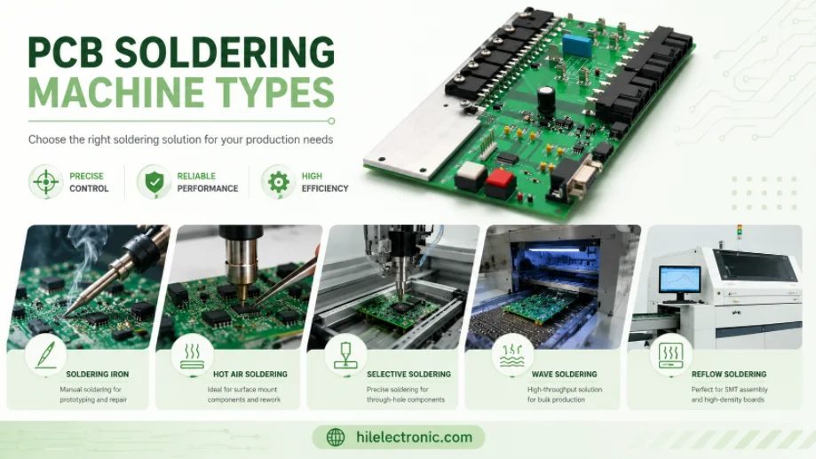
PCB Soldering Machine Types: Reflow, Wave, and Selective Equipment
Figure 1. PCB soldering machine types image for Highleap...
Clean Flux vs No-Clean Flux: Residue, Cleaning, and PCB Reliability
Figure 1. clean flux vs no-clean flux image for Highleap...
How to get a quote for PCBs
Let us run DFM/DFA analysis for you and get back to you with a report.
You can upload your files securely through our website.
We require the following information in order to give you a quote:
-
- Gerber, ODB++, or .pcb, spec.
- BOM list if you require assembly
- Quantity
- Turn time
In addition to PCB manufacturing, we offer a comprehensive range of electronic services, including PCB design, PCBA (Printed Circuit Board Assembly), and turnkey solutions. Whether you need help with prototyping, design verification, component sourcing, or mass production, we provide end-to-end support to ensure your project’s success. For PCBA services, please provide your BOM (Bill of Materials) and any specific assembly instructions. We also offer DFM/DFA analysis to optimize your designs for manufacturability and assembly, ensuring a smooth production process.