
Solder Balls in PCB Assembly – Manufacturing, Defects & Fixes

BGA Solder Balls
Definition and Basic Principles of Solder Balls
Solder balls, also known as solder spheres or solder bumps, are spherical solder granules primarily used for connecting PCBs and chip packages. In multi-chip modules, solder balls facilitate connections between stacked packages. Microscopically, solder balls form a metallic interconnect structure through a process of melting and solidification, ensuring reliable electrical and mechanical connections.
Manufacturing Processes of Solder Balls
Traditional Manufacturing Methods
Traditional solder ball manufacturing methods include continuous flow/quenching and reflow methods, typically following these steps:
- Material Preparation: Selection of suitable solder alloy such as Sn63Pb37 or lead-free solder.
- Shaping: Forming small pieces or granules through extrusion or cutting methods.
- Melting: Heating solder granules in a high-temperature oil column.
- Spheroidization: Utilizing surface tension principles to form molten solder into spherical shapes.
- Cooling: Cooling in a viscous liquid to maintain spherical integrity.
- Cleaning and Grading: Removing residues and classifying by size.
Advanced Manufacturing Technologies
Recent innovations in solder ball manufacturing have introduced new methods:
- Atomization Technology: Atomizing molten metal into tiny droplets using high-pressure gas, rapidly solidifying them into spherical shapes.
- 3D Printing: Utilizing metal 3D printing to directly manufacture precise-sized solder balls.
- Electroplating: Electrodepositing solder on minute conductive substrates to form uniform spherical structures.

Solder balls
Applications of Solder Balls
Ball Grid Array (BGA) Packaging
BGA remains one of the most widespread applications of solder balls. Compared to traditional Dual In-line Package (DIP) or flat packages, BGAs offer higher interconnect density and superior electrical performance. Advanced BGA technologies now support thousands of solder ball interconnections, meeting demands in high-performance computing and 5G communication fields.
3D Integrated Circuits
As Moore’s Law approaches physical limits, 3D integrated circuits represent a breakthrough technology. Solder balls play a crucial role in this domain, enabling higher integration and performance through vertical stacking and interconnecting multiple layers of chips.
Micro-Electro-Mechanical Systems (MEMS)
In MEMS devices, tiny solder balls facilitate precise mechanical and electrical connections, supporting various sensor and actuator functionalities.
Solder Ball Diameter Selection
Selecting the correct solder ball diameter is a crucial factor in PCB assembly, directly affecting electrical performance, mechanical strength, and reliability of solder joints. Engineers must carefully consider multiple factors to ensure optimal results.
Factors Influencing Solder Ball Diameter Selection
-
Package Type and Pitch: Fine-pitch packages require smaller solder balls to prevent bridging, while larger balls are suitable for high-power or coarse-pitch packages.
-
PCB Pad Size: The pad diameter must match the solder ball size to achieve proper wetting and joint formation.
-
Thermal Requirements: Larger solder balls improve heat dissipation for high-power devices, while smaller balls reduce thermal stress in compact assemblies.
-
Mechanical Reliability: Ball size impacts shear strength and resistance to mechanical stress during board handling or vibration.
-
Manufacturing Process: Reflow profile and solder alloy choice may influence the optimal diameter.
Typical Diameter Ranges
-
Small: 0.25–0.35 mm — suitable for ultra-fine-pitch BGAs or advanced miniaturized devices.
-
Medium: 0.36–0.50 mm — common in standard BGAs and CSPs.
-
Large: 0.51–0.76 mm — used in high-power modules or large-pitch packages.
Practical Recommendations
-
Verify compatibility with the PCB layout and pad design.
-
Consult IPC standards (such as IPC-7095) for reference diameters per package type.
-
Conduct prototype testing to confirm solder joint integrity before mass production.
Impact on Reliability and Quality Control
Proper solder ball diameter selection helps prevent common defects such as solder bridges, voids, or head-in-pillow issues. It also supports consistent thermal and electrical performance, making downstream quality control and reliability testing more predictable.
Quality Control and Reliability of Solder Balls
Key Parameters
- Dimensional Uniformity: Directly impacts interconnection consistency and reliability.
- Alloy Composition: Determines solder ball melting point, strength, and conductivity.
- Surface Oxidation Level: Affects soldering performance and long-term reliability.
Advanced Inspection Methods
- X-ray Inspection: Non-destructive examination of internal structure and arrangement of solder balls.
- Atomic Force Microscopy (AFM): Analysis of surface morphology and microstructure of solder balls.
- Thermal Imaging: Evaluation of thermal performance and potential defects in solder ball connections.
Technologies for Enhanced Reliability
Research indicates that adding a thin film of Palladium (Pd) at the solder ball interface significantly improves solder joint reliability. Recent data shows that Pd films ranging from 0.02 to 0.05 micrometers perform optimally even after multiple reflows, surpassing traditional electroless Ni/Au processes.

BGA solder joint and solder ball inspection (Source: XVoid AI, xray-lab.com)
Defects in Solder Balls and Solutions
Common Defects
- Solder Ball Loss: Due to poor soldering or mechanical stress causing balls to detach from pads.
- Solder Bridges: Unnecessary connections formed between adjacent solder balls.
- Voids: Formation of bubbles inside solder balls, reducing connection strength and conductivity.
Advanced Defect Prevention Technologies
- Plasma Cleaning: Pre-treatment of PCB surfaces with plasma before soldering to enhance soldering performance.
- Vacuum Reflow: Application of a vacuum environment during reflow to minimize void formation inside solder balls.
- Intelligent Temperature Profile Control: Utilization of AI algorithms to optimize reflow temperature profiles, enhancing soldering quality.
Future Trends in Solder Ball Technology
Nanoscale Solder Balls
With ongoing miniaturization of electronic devices, researchers are developing nanoscale solder ball technologies. These tiny solder balls enable higher interconnect densities while presenting new challenges such as quantum effects and surface tension-dominated behaviors.
Environmentally Friendly Solder Materials
To comply with environmental regulations, ongoing research focuses on lead-free solder material development. The latest alloy formulations not only meet environmental requirements but also offer performance comparable to or better than traditional lead-containing solders.
Self-Repairing Solder Balls
Inspired by biological principles, researchers are exploring solder ball materials capable of self-repair. These materials automatically heal microcracks, significantly enhancing the lifespan and reliability of electronic products.
Conclusion
Solder ball technology, as a core of electronic manufacturing, is undergoing rapid innovation and development. From traditional interconnection methods to advanced 3D integration, solder balls play an irreplaceable role in advancing electronic technology. With the emergence of new materials, processes, and applications, solder ball technology will continue to evolve, paving the way for smaller, faster, and more reliable electronic devices.
Understanding all aspects of solder ball technology is crucial for electronic engineers and researchers. By continually optimizing manufacturing processes, improving quality control, and exploring new applications, we can fully harness the potential of solder ball technology to drive forward the entire electronics industry.
FAQ
- What are the considerations for selecting the optimal solder ball diameter for different PCB applications?The diameter of solder balls directly impacts the mechanical and electrical performance of PCB assemblies. Factors such as thermal management, interconnect density, and package size influence the choice of solder ball diameter. Selecting the right diameter ensures efficient heat dissipation and reliable electrical connections in diverse electronic applications.
- How does the surface tension of molten solder affect the formation of solder balls during the manufacturing process?Surface tension plays a critical role in shaping molten solder into spherical balls. Understanding this phenomenon is essential for optimizing manufacturing techniques like atomization and 3D printing. Manipulating surface tension allows precise control over solder ball formation, ensuring uniformity and reliability in electronic assemblies.
- What advancements are being made in the integration of solder balls for emerging flexible electronics applications?Flexible electronics demand unique soldering solutions due to their bendable substrates and varied form factors. Innovations in solder ball integration techniques cater to these requirements, enabling robust connections that withstand mechanical strain and environmental conditions. These advancements support the evolution of wearable technology and foldable displays.
- How do environmental factors, such as humidity and temperature fluctuations, impact the long-term reliability of solder ball connections?Environmental conditions significantly influence the performance of solder ball connections over time. Variations in humidity and temperature can accelerate oxidation or induce thermal expansion mismatches, potentially compromising solder joint integrity. Implementing protective coatings or alloy enhancements mitigates these effects, ensuring sustained reliability in diverse operating environments.
- What role do solder balls play in enhancing the energy efficiency of next-generation electronic devices?Solder balls contribute to improving the energy efficiency of electronic devices through enhanced thermal management and reduced electrical resistance. Their efficient heat dissipation properties and optimized electrical conductivity support the development of power-efficient processors and components. This efficiency enhancement is crucial for advancing technologies in smart grids and IoT applications.

Related Articles

Clean Flux vs No-Clean Flux: Residue, Cleaning, and PCB Reliability
Figure 1. clean flux vs no-clean flux image for Highleap...
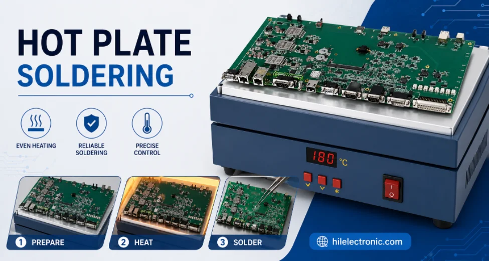
Hot Plate Soldering: Process, Limits, and Reflow Comparison
Figure 1. hot plate soldering image for Highleap...
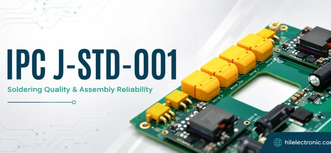
IPC J-STD-001: Classes, Requirements, and RFQ Specification
Figure 1. IPC J-STD-001 image for Highleap Electronics PCB...
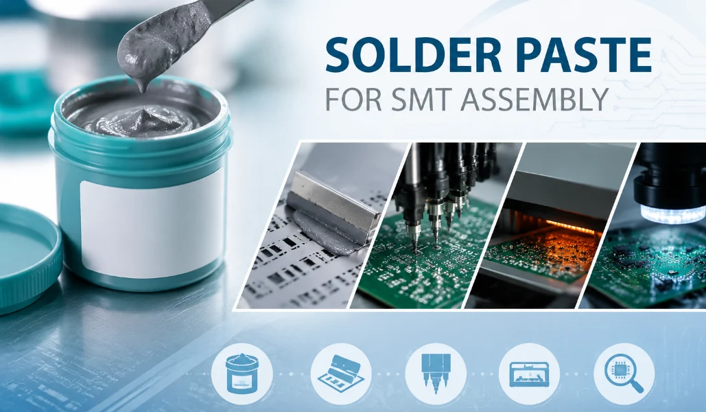
Solder Paste for SMT Assembly: Types, Storage, and Printing Defects
Figure 1. Solder paste selection affects SMT print...
How to get a quote for PCBs
Let us run DFM/DFA analysis for you and get back to you with a report.
You can upload your files securely through our website.
We require the following information in order to give you a quote:
-
- Gerber, ODB++, or .pcb, spec.
- BOM list if you require assembly
- Quantity
- Turn time
In addition to PCB manufacturing, we offer a comprehensive range of electronic services, including PCB design, PCBA (Printed Circuit Board Assembly), and turnkey solutions. Whether you need help with prototyping, design verification, component sourcing, or mass production, we provide end-to-end support to ensure your project’s success. For PCBA services, please provide your BOM (Bill of Materials) and any specific assembly instructions. We also offer DFM/DFA analysis to optimize your designs for manufacturability and assembly, ensuring a smooth production process.