
Back to blog
What Does Solder Mask Bridge Mean and How Can You Prevent It?

What is a solder mask bridge?
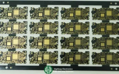
A solder mask bridge refers to an unintended connection or continuity of solder mask material between two adjacent conductive elements or pads on a PCB. The solder mask is a protective layer applied over the copper traces and pads on a PCB to prevent solder from flowing where it is not intended during the soldering process.
During PCB fabrication, the solder mask is typically applied to cover the entire board surface, leaving openings or “windows” only where solder pads or exposed copper traces are located. However, in some cases, due to manufacturing errors or design issues, the solder mask may extend beyond the intended area and create a bridge or connection between adjacent pads or traces.
Solder mask bridges can cause short circuits or interference between neighboring conductive elements, leading to electrical malfunctions or failures in the circuit. They can be problematic, especially in high-density designs where the spacing between pads or traces is minimal.
To prevent solder mask bridges, proper design guidelines, manufacturing processes, and quality control measures should be followed. Designers should ensure sufficient spacing between adjacent pads, use appropriate solder mask relief or expansion values, and perform thorough inspections and testing during PCB manufacturing to detect and rectify any potential solder mask bridging issues.
How your PCB is impacted by the solder masking process

The solder masking process plays a crucial role in the fabrication and performance of printed circuit boards (PCBs). Here’s how the solder masking process impacts your PCB:
- Prevents Solder Mask Bridges: One of the primary functions of the solder mask is to prevent solder mask bridges. It creates a barrier or “solder dam” between solder joints and other conductive areas of the board. This prevents unintended connections between conductive elements, which could lead to board damage or short circuits. Solder mask bridges are a common issue during PCB assembly, and the solder mask helps mitigate this problem.
- Reduces Solder Paste Consumption: Solder paste is used during the soldering process to create electrical connections. The solder mask reduces the need for excessive solder paste by providing insulation between the board’s components. This not only saves on material costs but also helps prevent solder-related defects.
- Safeguards the PCB: The solder mask serves as a protective layer that shields the PCB from contaminants that may be introduced during handling or assembly. It acts as a barrier, preventing dust, dirt, moisture, and other pollutants from coming into contact with the conductive elements on the board’s surface. This protection can extend the operational lifetime of the device.
- Increases Breakdown Voltage: The dielectric material used in PCBs has a breakdown voltage, which is the maximum voltage it can withstand before electrical arcing occurs. By applying the solder mask, you can improve the breakdown voltage of the PCB. This is especially important for high-voltage boards (over 1 kV), as it provides additional protection against corona discharge and electrical arcs.
- Prevents Metal Whisker Formation: Metal whiskers are tiny, hair-like structures that can grow on the surface of certain metals, including tin. They can cause electrical shorts and other problems in electronic components. The solder mask helps prevent the development of tin whiskers, particularly in components with lead-free solder and tin plating. By acting as a barrier, the solder mask reduces the risk of whisker formation.
Overall, the solder masking process is essential for ensuring the reliability and performance of PCBs. It addresses various issues, including preventing solder mask bridges, reducing solder paste consumption, protecting the PCB from contaminants, enhancing breakdown voltage, and minimizing the risk of metal whisker formation. While there may be cases where a solder mask is not feasible, it is generally a critical step in PCB manufacturing to ensure the functionality and longevity of electronic devices. Consulting with your PCB manufacturer (CM) is advisable to assess the specific requirements and consequences of solder mask application for your PCB design.
Commonly Known Issues of Soldering Bridging
Solder bridging during soldering can lead to several commonly known issues, including:
Dewetting and Non-Wetting: Dewetting occurs when molten solder initially covers a pad but then retreats, leaving a solder mound. Non-wetting, on the other hand, happens when the molten solder does not properly wet the exposed copper on the pad. These issues can arise due to inadequate plating on brass components or the need to change the flux.
Pin Holes and Blow Holes: Pin holes and blow holes are defects that occur when there are poor copper plating or excessive moisture on the board. Pin holes are tiny voids or gaps in the solder joint, while blow holes are larger voids or cavities caused by trapped moisture or gases.
Lifted Pads: Lifted pads occur when the soldered component is removed and the soldering surface has worn-out or uneven copper plating. This can result in the pads detaching from the PCB, causing electrical connection issues.
Tombstone: Tombstoning happens during wave soldering when a component is lifted and stands vertically, resembling a tombstone. It can be caused by using components with different solderability characteristics or using leads of incorrect lengths.
Excess Solder: Excessive solder accumulation can occur due to factors such as improper lead size compared to the pad ratio or the rapid movement of the conveyor belt during the soldering process. This can lead to solder bridges and poor solder joint quality.
These issues can affect the functionality, reliability, and performance of the soldered connections on the PCB. To mitigate these problems, it is important to follow proper soldering techniques, ensure adequate plating and cleanliness of the board, and use components that are compatible with the soldering process. Additionally, inspection and quality control measures should be implemented to detect and address any soldering defects before the PCB is used in electronic devices.
What You Must Do To Avoid Solder Mask Bridges?
To avoid solder mask bridges in your PCB assembly, you can follow a set of precautions and best practices throughout the design, manufacturing, and assembly processes. Here are the key steps to prevent solder mask bridges:
- Verify PCB Design: Carefully review your PCB design to ensure that it meets the best practices for manufacturability, especially for surface mount and through-hole components. Following industry standards like those defined by the IPC (Institute for Printed Circuits) can help ensure high-quality design.

- Design Rules for Mask Relief: Check the design rules for mask relief, especially for areas where solder mask application is not required. Set the relief values to appropriate dimensions, typically between 0.003 to 0.008 inches for SMT (Surface Mount Technology) components. Adjust these values as needed, particularly when working with closely spaced pads.
- Alter Reflow Profile: Modify the reflow profile during the soldering process. Lengthen the time at temperatures just above the solder’s melting point to allow pads and component leads to reach the desired temperature gradually. This gradual heating promotes proper wetting and adhesion without creating solder bridges.
- Use Solder Mask Dams: Implement solder mask dams between SMT pads. These dams act as isolation walls to prevent solder from spreading beyond the intended areas. Ensure that the minimum size of the dam is adequate, typically around 0.004 inches. Adjust this size based on specific design requirements.
- Consider Lead Length for Through-Hole Components: For through-hole components, consider the appropriate lead length. Factors like board thickness, component size, and soldering method can influence the required lead length. Consult with your PCB manufacturer to determine the correct length to avoid bridging.
- Minimize Solder Paste Volume: Overuse of solder paste can lead to solder mask bridges. Reduce the volume of solder paste applied to the board or adjust the stencil design to control the paste application location, especially in areas with small spacing between components.
- Utilize Solder Mask Specified Pads: In tight or challenging regions where solder mask dams are not feasible, you can use solder-mask-defined pads to protect the soldering surface. This approach helps prevent solder mask bridges in confined spaces.
- Proper Pad Diameter and Hole Size: Ensure that you use the appropriate pad diameter and hole size in your PCB design. Larger copper pads or through holes between closely spaced surfaces increase the risk of solder mask bridges.
- Apply Solder Masking Properly: The application of the solder mask is critical. Ensure that the solder mask is applied in areas where soldering is not required. Solder mask materials, typically epoxy-based, prevent molten solder from sticking to them, helping prevent solder mask bridges.
- Utilize Fiducials: Include fiducial markers on your PCB design. These fiducials aid in precise automated component placement and alignment during assembly. Accurate component placement reduces the chances of misaligned components that could lead to solder mask bridges.
- Collaborate with a Reputable PCB Manufacturer: Partner with an experienced and reputable PCB manufacturer. Communicate your design requirements, including the need to prevent solder mask bridges, and work closely with the manufacturer to ensure that best practices are followed throughout the fabrication and assembly processes.
By following these precautions and working collaboratively with your PCB manufacturer, you can significantly reduce the risk of solder mask bridges and ensure the quality and reliability of your PCB assemblies.
How You can Fix the Solder mask bridges
Fixing solder mask bridges is a delicate process that requires the use of proper tools and techniques. Here’s how you can fix solder mask bridges step by step:
Tools and Materials Needed:
- Soldering iron with a fine tip and adjustable temperature control
- Solder wick (desoldering braid)
- Solder flux
- Multimeter (optional, for testing)
- Wet sponge or damp cloth (for cleaning the soldering iron tip)
Procedure:
- Prepare Your Soldering Iron: Set the temperature on your soldering iron to a suitable value, typically around 150-250°C (300-480°F), depending on the solder and components used. Allow the iron to fully reach this temperature before proceeding.
- Monitor Temperature: Ensure that the soldering iron tip reaches the required temperature for soldering. You may need to increase the temperature by a few degrees to account for heat absorption by the solder wick during the repair process. For example, if you are soldering at 250°C, you can set the iron to 270°C.
- Use Surface Tension: In some cases, you can use the surface tension of the molten solder to detach the solder mask bridge without the need for a wick. To do this, gently touch the solder bridge with the tip of the soldering iron. The surface tension should pull the excess solder away from the bridged area. Be careful not to overheat the PCB or components.
- Utilize Solder Wick: If using surface tension alone doesn’t remove the bridge, you can proceed with using solder wick (desoldering braid). Here’s how to do it:
- Apply a small amount of solder flux to the solder mask bridge. This will help with solder flow and absorption.
- Position the solder wick directly over the bridge, ensuring it covers the entire bridged area.
- Place the soldering iron tip on top of the wick, applying gentle pressure to transfer heat.
- The heat will cause the solder on the bridge to melt and be absorbed into the wick. Move the iron slowly to cover the entire bridge area.
- Replace Clogged Wick (if necessary): If the solder wick becomes clogged with absorbed solder, replace it with a fresh section to continue the process effectively.
- Clean the Soldering Iron Tip: Periodically, clean the tip of the soldering iron by wiping it on a wet sponge or damp cloth. A clean tip ensures good heat transfer during the repair.
- Inspect the Repair: After removing the solder mask bridge, inspect the area to ensure that it is clean and free from solder bridges. You may also want to test for continuity between the previously bridged points using a multimeter in continuity mode.
- Reapply Solder (if necessary): If removing the bridge results in the removal of the solder joint, apply additional solder to reestablish a clean and solid solder connection between the components.
Remember to exercise caution and precision during the solder mask bridge repair process to avoid damaging the PCB or components. If you are not confident in your soldering skills, consider seeking assistance from a skilled technician or a professional electronics repair service.
conclusion
Overall, solder mask bridges can be detrimental to circuit boards due to the potential for electrical shorts. It is important to follow the preventive measures mentioned earlier to avoid their occurrence. However, if solder mask bridges do occur, it is necessary to address them promptly. This can involve carefully inspecting the affected areas, removing excess solder using appropriate tools like solder wick or a solder sucker, and ensuring proper solder joint reflow or rework. If needed, consulting with an experienced technician or PCB manufacturer can provide guidance and assistance in resolving solder mask bridge issues effectively. By taking quick action, you can mitigate the potential negative impact of solder mask bridges on your circuit boards.

Related Articles
High-Quality Rigid PCB Circuit Board Fabrication Services
Rigid PCBs are the conventional type of FR4 PCB, comprising a rigid substrate typically made of materials like fiberglass.

PCB Mounting Holes: Understanding Counterbore and Countersink
The choice between countersink and counterbore holes depends on various factors, including the type of screw and the application requirements.
Common PCB Drilling Process Faults and Solutions
This article discusses common PCB drilling process faults, their causes, and solutions to ensure a smooth and efficient drilling process.