
Surface Finish for RF and Microwave PCBs: A Technical Comparison for High-Frequency Applications

Introduction
Surface Finish for RF and Microwave PCBs directly affects high-frequency conductor loss and soldering reliability; choosing the right finish is therefore critical for antenna feeds, mmWave traces and RF connectors. In the GHz frequency range and beyond, seemingly minor variations in surface conductivity, roughness, and contact resistance translate into measurable degradation in insertion loss, return loss, and passive intermodulation performance.
The central challenge facing RF engineers is balancing electrical performance against manufacturing reliability: ultra-smooth finishes may optimize signal integrity but complicate assembly, while robust solderable coatings can introduce unacceptable losses above 10 GHz. This article systematically compares common PCB surface treatments and provides frequency-specific recommendations for antenna structures, transmission lines, connectors, waveguide interfaces, and wire-bonding areas.
High-Frequency Loss Mechanisms in RF PCB Surface Finishes
Skin Depth and Current Concentration
At microwave frequencies, alternating current concentrates near the conductor surface due to the skin effect. Skin depth δ follows the relationship δ = √(2 / ωμσ), where ω is angular frequency, μ is permeability, and σ is conductivity. At 1 GHz in copper, skin depth measures approximately 2.1 μm; at 30 GHz it shrinks to 0.38 μm. This exponential decrease forces high-frequency currents into a thin surface layer, making surface finish quality paramount for RF and microwave PCB performance.
Surface Roughness Impact on RF Loss
Surface roughness increases the effective current path length beyond the nominal trace geometry. The Hammerstad-Jensen model quantifies this effect through a roughness correction factor that adds to conductor loss. RMS roughness values above 1 μm can increase attenuation by 20-40% at mmWave frequencies.
Chemical surface finishes typically exhibit Ra values of 0.3-0.8 μm, while hot-air leveled surfaces often exceed 2 μm. This difference becomes critical when selecting surface finish for RF applications above 10 GHz.
Plating Layer Material Conductivity
Electrodeposited and immersion-plated layers introduce materials with different conductivities than base copper. Nickel (1.43×10⁷ S/m) conducts approximately four times worse than copper (5.96×10⁷ S/m), while gold (4.10×10⁷ S/m) and silver (6.30×10⁷ S/m) approach copper’s performance.
Layer thickness becomes critical for RF PCB surface finish selection: nickel barriers thicker than the skin depth directly contribute to RF resistance, while ultrathin gold flash layers oxidize rapidly without adequate thickness (minimum 0.05 μm recommended).
Contact Resistance at RF Interconnects
At connector interfaces, edge contacts, and coaxial-to-PCB transitions, contact resistance and passivation layers dominate loss mechanisms. Oxide formation on exposed metals increases junction resistance, generating both linear loss and passive intermodulation products. Hard gold platings on edge fingers maintain low contact resistance through repeated insertions, while soft finishes degrade rapidly under mechanical stress.

Common PCB Surface Finish Types for RF Applications
HASL (Hot Air Solder Leveling)
-
Excellent solderability at low cost – Tin-based coating provides robust wetting for standard SMT assembly and multiple reflow cycles.
-
High surface roughness – Air-knife leveling produces >2–3 μm RMS roughness, significantly increasing conductor loss above 3 GHz.
-
Use case – Suitable for non-critical RF areas, power planes, and cost-sensitive designs where RF path area is minimal.
ENIG (Electroless Nickel Immersion Gold)
-
Flat and solderable surface – Nickel (3–6 μm) with a thin gold layer (0.05–0.15 μm) ensures planarity and oxidation resistance.
-
Moderate roughness – Surface smoothness of 0.4–0.7 μm provides good RF performance through ~20 GHz.
-
Potential issue – “Black pad” defects from excess phosphorus in nickel are preventable with proper process control (IPC-4552).
-
Performance range – Ideal for general RF and microwave PCBs where cost and reliability must be balanced.
ENEPIG (Electroless Nickel Electroless Palladium Immersion Gold)
-
Enhanced interface stability – Palladium barrier (0.05–0.15 μm) protects nickel from corrosion and prevents black-pad formation.
-
Superior reliability – Supports both reflow soldering and wire bonding in mixed-technology assemblies.
-
Low RF loss – Palladium introduces minimal insertion loss, suitable for high-frequency designs up to Ka-band (26–40 GHz).
-
Cost factor – 20–30% higher than ENIG, justified by reliability and bonding flexibility.
Immersion Silver
-
High conductivity – Silver (6.30×10⁷ S/m) closely matches copper, ensuring minimal conductor loss.
-
Smooth surface – Roughness typically 0.3–0.5 μm, excellent for high-frequency signal transmission.
-
Tarnish risk – Sulfide formation can increase resistance; controlled storage and anti-tarnish packaging are essential.
-
Application – Preferred for microwave transmission lines and antenna traces prioritizing electrical performance.
Immersion Tin
-
Flat and cost-effective – 0.8–1.2 μm tin coating directly over copper provides reliable solderability and moderate cost.
-
Microwave capability – Performs well up to X-band (8–12 GHz) with acceptable insertion loss.
-
Tin whisker risk – Modern grain refiners mitigate, but do not eliminate, whisker formation under stress.
-
Use case – Suitable for medium-frequency RF designs with predictable, short assembly cycles.
OSP (Organic Solderability Preservative)
-
Lowest theoretical RF loss – No metallic layer; copper remains the sole conductive surface.
-
Thin protective film – 0.2–0.5 μm organic coating prevents oxidation while maintaining RF integrity.
-
Limited durability – Sensitive to handling, supports typically one reflow, and has 6–12 month shelf life.
-
Best for rapid-turn builds – Ideal for high-frequency PCBs with fast production and minimal storage time.
Hard Gold for RF Connectors
-
High wear resistance – Electroplated gold (0.5–2.5 μm) over nickel (3–5 μm) ensures long mechanical life.
-
Stable electrical contact – Maintains contact resistance below 10 mΩ even after thousands of insertion cycles.
-
Cost-efficient application – Used selectively on connector edges and test points; solderable zones often use ENIG.
-
Preferred for RF interfaces – Ensures low-loss, stable signal transfer in coaxial and edge-launch connectors.
Frequency-Specific Surface Finish Recommendations for RF PCBs
Below 3 GHz Applications
At frequencies below 3 GHz, skin depth exceeds 1 μm and surface finish selection centers on soldering reliability and cost rather than electrical performance. ENIG, immersion silver, immersion tin, and even lead-free HASL on non-critical traces all provide acceptable RF performance.
Standard manufacturing considerations dominate: ENIG offers the best balance of solderability, flatness, and shelf life for mixed-signal boards. Surface finish choice in this range should align with assembly capabilities and volume economics rather than marginal electrical differences.
3-20 GHz Mid-Microwave Range
Mid-microwave frequencies demand attention to surface roughness while maintaining solderable surfaces for component assembly. ENIG and immersion silver emerge as preferred surface finishes for RF and microwave PCBs, with typical insertion loss differences below 0.1 dB/inch for well-executed finishes.
ENIG provides superior process maturity and wider supplier capability, while immersion silver offers marginally better electrical performance with increased storage sensitivity. HASL should be excluded from RF transmission paths in this frequency range due to excessive roughness-induced loss.
Above 30 GHz Millimeter-Wave Applications
Millimeter-wave applications face extreme sensitivity to surface roughness and plating thickness variations. Skin depth at 30 GHz measures only 0.38 μm in copper, forcing current into surface irregularities and plating layers.
Ultra-smooth ENIG with controlled nickel thickness (3-4 μm maximum) or immersion silver provides the most practical solutions for solderable surfaces. Where soldering is unnecessary, such as antenna radiators or probe-fed structures, bare copper with protective encapsulation or precision hard gold plating on critical contact areas minimizes loss. At these frequencies, substrate loss tangent typically dominates total insertion loss, but surface finish optimization remains essential.

RF & Microwave PCBs
Soldering Reliability and Thermomechanical Performance
Intermetallic Compound Formation
Solder joint reliability depends on controlled intermetallic compound formation at the solder-finish interface. ENIG and ENEPIG form Cu-Sn and Ni-Sn IMC layers during reflow, with proper gold thickness (0.05-0.10 μm) ensuring complete gold dissolution into solder without leaving residual layers that embrittle joints.
Excessive gold thickness creates gold-tin intermetallics with inferior mechanical properties. Immersion silver forms Cu-Sn IMC directly, producing strong joints but requiring rapid reflow to prevent excessive silver dissolution.
Thermal Cycling Behavior
Coefficient of thermal expansion mismatches between copper, nickel plating, and gold create interfacial stress during temperature cycling. ENIG and ENEPIG withstand hundreds of thermal cycles without delamination when properly processed. Immersion silver demonstrates excellent thermal cycling performance with direct copper bonding.
Immersion tin faces potential tin whisker formation accelerated by thermal stress, requiring risk assessment in high-reliability applications. Multiple reflow exposures progressively degrade all surface finishes through oxidation and IMC growth.
Reflow Profile Compatibility
Peak reflow temperatures for lead-free solder (typically 245-255°C for 40-90 seconds above 217°C) must not damage surface finishes or promote excessive IMC formation. The following compatibility guidelines apply:
- ENIG and ENEPIG – Tolerate multiple reflows without degradation, supporting complex assemblies with sequential reflow operations.
- Immersion silver – Typically supports 2-3 reflows before oxidation degrades solderability; nitrogen atmosphere recommended.
- OSP – Coatings decompose partially during reflow; single reflow represents best practice for RF applications.
- Immersion tin – Maintains solderability through multiple reflows but faces accelerated whisker nucleation from thermal stress.
Testing and Validation of RF PCB Surface Finishes
S-Parameter Measurement and Loss Characterization
Insertion loss verification requires calibrated vector network analyzer measurements of representative transmission line structures across the operating frequency range. Test structures should include 50-ohm microstrip or stripline traces at least 3 inches long with identical geometries across finish variants.
Time-domain reflectometry reveals impedance discontinuities at finish transitions, while frequency-domain S21 measurements quantify total loss. Comparing measured results against electromagnetic simulation using finish-specific surface roughness parameters validates models and identifies process outliers.
Surface Characterization Methods
Surface roughness measurement employs optical profilometry or atomic force microscopy to quantify Ra, Rq, and profile parameters that feed electromagnetic simulation tools. Cross-sectional microscopy reveals finish thickness, IMC formation, and interface integrity.
Scanning electron microscopy identifies grain structure, contamination, and defects below optical resolution limits. These measurements establish baseline characteristics for incoming material qualification and process control of surface finish for RF applications.
Reliability and Environmental Testing
Accelerated life testing subjects finished boards to thermal cycling, humidity exposure, and salt-fog environments per IPC-TM-650 test methods. Solder joint strength measurement through shear and pull testing validates assembly reliability across finish types.
For critical RF applications, passive intermodulation testing identifies nonlinear junction behavior that generates interference in receive bands. Contact resistance measurement at RF connector interfaces before and after insertion cycling validates wear performance of edge gold.

Design and Manufacturing Best Practices for RF Surface Finish Selection
Specification and Documentation Requirements
Manufacturing drawings must explicitly specify surface finish type, applicable areas, and critical parameters. IPC-4552 for ENIG and IPC-4553 for ENEPIG provide standardized classifications. Required specifications include:
- Gold thickness – ENIG: 0.05-0.15 μm; Hard gold: 0.5-2.5 μm
- Nickel thickness – 3-6 μm typical; 3-4 μm maximum for mmWave applications
- Phosphorus content – Nickel: 6-9% for optimal ductility and corrosion resistance
- Surface roughness limits – Ra < 0.8 μm for RF traces; Ra < 0.5 μm for mmWave
Separate finish callouts for RF transmission paths, solderable component areas, and connector contacts enable optimized performance in each functional zone.
Fabrication Process Optimization
Post-etch copper surface preparation significantly impacts final finish quality. Mechanical scrubbing should be minimized or eliminated on RF transmission lines, replaced with chemical cleaning that preserves surface smoothness.
For immersion finishes, bath chemistry control and temperature stability directly affect uniformity and adhesion. Specification of reverse-treat-foil or very-low-profile copper reduces baseline roughness before finish application. Clear communication with fabricators regarding RF-critical areas enables appropriate handling and process attention.
Selective Finish Application Strategies
Cost optimization and performance maximization both benefit from selective finish application. Hard gold on edge contacts and connector interfaces provides durability where needed without incurring cost across the entire board.
ENIG or immersion silver on RF traces ensures signal integrity, while standard ENIG or immersion tin suffices for power and control circuitry. This approach requires careful masking and process sequencing but delivers optimal cost-performance balance for RF and microwave PCB assemblies.
Supplier Quality Requirements
Contractual specifications should reference applicable IPC standards and define acceptance testing for critical parameters. For base station and antenna applications, require passive intermodulation testing of representative assemblies to verify finish quality and cleanliness.
Surface finish thickness measurement on test coupons traveling with production panels verifies process control. Incoming inspection protocols should include visual examination for discoloration, adhesion testing per IPC-TM-650, and electrical continuity verification.
Conclusion: Optimizing Surface Finish for RF and Microwave PCB Performance
Surface finish selection for RF and microwave PCBs demands careful evaluation of electrical performance against manufacturing practicality. At frequencies above 3 GHz, surface smoothness and conductor quality directly impact insertion loss and system performance, making finish selection a critical design parameter rather than a manufacturing afterthought.
ENIG provides the most versatile solution across frequency ranges and assembly processes, while immersion silver optimizes electrical performance at the cost of storage sensitivity. ENEPIG addresses high-reliability requirements where wire bonding or extreme environmental exposure demands maximum interface stability.
Highleap Electronics RF PCB Surface Finish Capabilities
Highleap Electronics maintains comprehensive surface finish capabilities specifically engineered for RF and microwave applications:
- ENIG processing – IPC-4552 Class 2 and 3 with documented nickel thickness control (3-6 μm) and gold thickness verification (0.05-0.15 μm) for optimal high-frequency performance
- ENEPIG for mixed assembly – Supporting both reflow soldering and gold/aluminum wire bonding with palladium barrier protection for maximum reliability
- Immersion silver – Controlled deposition processes with anti-tarnish packaging and documented surface roughness below 0.5 μm Ra for microwave applications
- Selective hard gold plating – Edge connector and RF contact finishing with cobalt-hardened gold for insertion durability and low contact resistance
- Quality verification – S-parameter test coupons on production panels, surface roughness measurement, cross-sectional analysis, and PIM testing capabilities
Our engineering team provides surface finish consultation including electromagnetic simulation correlation, thermal cycling validation, and frequency-specific optimization recommendations. We work directly with RF design teams to balance electrical performance requirements against assembly process constraints and cost targets.
Contact Highleap Electronics today to discuss surface finish optimization for your RF and microwave PCB project. Our technical specialists will review your frequency range, assembly requirements, and performance targets to recommend the optimal finish strategy for your application.

Recommended Posts

NP-175F PCB Laminate for High-Reliability Multilayer Boards
NP-175F PCB laminate is a Nan Ya high-Tg, filled...

High CTI FR-4 PCB Manufacturing for Insulation-Critical Boards
High CTI FR-4 is used when a PCB design needs stronger...
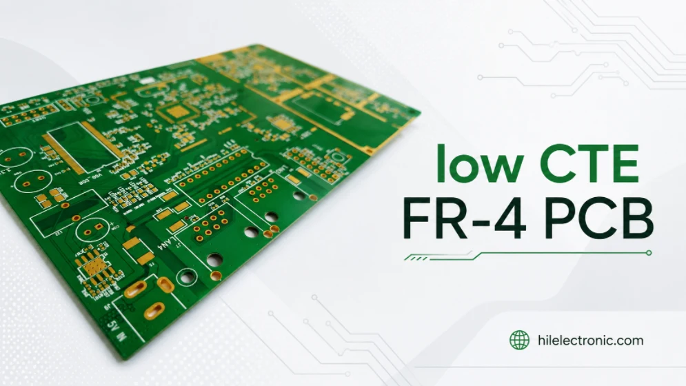
Low CTE FR-4 PCB Manufacturing for Through-Hole Reliability
Low CTE FR-4 PCB manufacturing is used when a circuit...
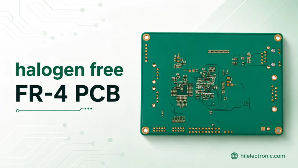
Halogen Free FR-4 PCB Manufacturing for Controlled Material Builds
Halogen free FR-4 PCB manufacturing is used when a product...
How to get a quote for PCBs
Let‘s run DFM/DFA analysis for you and get back to you with a report. You can upload your files securely through our website. We require the following information in order to give you a quote:
-
- Gerber, ODB++, or .pcb, spec.
- BOM list if you require assembly
- Quantity
- Turn time
In addition to PCB manufacturing, we offer a comprehensive range of electronic services, including PCB design, PCBA, and turnkey solutions. Whether you need help with prototyping, design verification, component sourcing, or mass production, we provide end-to-end support to ensure your project’s success.
For PCBA services, please provide your BOM (Bill of Materials) and any specific assembly instructions. We also offer DFM/DFA analysis to optimize your designs for manufacturability and assembly, ensuring a smooth production process.