
Back to blog
Exploring the World of Ultra-Thin PCBs

What is Ultra-Thin PCBs
Ultra-Thin Printed Circuit Boards (PCBs) are at the cutting edge of PCB technology, pushing the boundaries of electronics miniaturization and flexibility. These PCBs, defined by their exceptionally low profile, typically measure less than half the thickness of standard PCBs, often falling in the range of a few millimeters or less. This dramatic reduction in thickness heralds a new era in electronic design and functionality.
The genesis of ultra-thin PCBs is rooted in the growing demand for more compact and versatile electronic devices. As consumer electronics, medical devices, and wearable technology continue to evolve, the need for smaller, lighter, and more flexible components becomes paramount. Ultra-thin PCBs answer this call, offering a solution that traditional PCBs, with their relative bulk and rigidity, cannot provide.
Key Applications of Ultra-Thin PCBs
- Wearable Technology: Ultra-thin PCBs are ideal for wearables due to their lightweight and flexible nature, allowing for comfortable and unobtrusive designs.
- Smartphones and Portable Devices: Their thin profile enables slimmer, more compact designs in smartphones and other portable electronics, enhancing portability and aesthetic appeal.
- Medical Devices: In medical applications, ultra-thin PCBs offer the necessary compactness and flexibility for small, sophisticated devices like implants and monitoring systems.
- Flexible Electronics: The flexibility of ultra-thin PCBs makes them perfect for innovative applications in flexible screens, foldable devices, and other emerging technologies.
- Aerospace and Automotive Industries: Their reduced weight and size are beneficial in aerospace and automotive applications, where space optimization and weight reduction are critical.
Advantages of Ultra-Thin PCBs
Enhanced Flexibility and Compactness
Ultra-thin PCBs are highly valued for their flexibility, enabling the development of cutting-edge designs in space-constrained applications. Their thin, flexible nature makes them particularly well-suited for wearable devices, foldable electronics, and other compact systems that require adaptability in tight spaces. The ability to bend without compromising functionality opens up new opportunities for innovative form factors in modern consumer electronics and advanced technologies like flexible displays and medical devices.
Lightweight Nature
The reduced material volume of ultra-thin PCBs results in a significantly lighter end product. This is especially critical in industries where portability is a priority, such as in smartphones, tablets, wearables, and drones. A lighter PCB not only improves user comfort but also enhances the overall performance of mobile devices by minimizing the load on battery life and ensuring easier handling.
Improved Heat Dissipation
Despite their thin profile, ultra-thin PCBs can provide excellent heat dissipation properties. The reduced thickness of the board allows for better thermal conductivity, helping to dissipate heat more efficiently from components that generate high amounts of heat. This is especially important in high-performance devices like power electronics, high-speed processors, and LED lighting systems, where managing heat is crucial for maintaining optimal operation and extending the lifespan of the device.
Greater Design Versatility
Ultra-thin PCBs offer greater flexibility in design, allowing engineers to create compact, highly integrated layouts that would be challenging with thicker PCBs. Their ability to accommodate smaller, more complex circuits makes them ideal for applications in emerging fields like Internet of Things (IoT) devices, medical implants, and miniaturized consumer electronics. Designers can integrate more functionality into smaller spaces, optimizing the performance and efficiency of their products while keeping the overall size to a minimum.
Reduced Environmental Impact
By using fewer materials in their construction, ultra-thin PCBs are an environmentally friendly option in electronics manufacturing. Their lightweight and compact nature not only reduces the amount of raw materials needed but also minimizes waste, aligning with sustainability efforts in the electronics industry. This reduction in material usage and the potential for more efficient recycling processes make ultra-thin PCBs an attractive option for companies focused on reducing their environmental footprint and supporting green manufacturing initiatives.
Ultra-thin PCBs offer a range of advantages that make them an ideal choice for modern electronic devices. From enhancing portability and flexibility to improving heat dissipation and contributing to environmental sustainability, ultra-thin PCBs are driving innovation in industries across the globe.
Challenges and Limitations of Ultra-Thin PCBs
While ultra-thin PCBs offer numerous benefits, they also present specific challenges and limitations in their design, manufacturing, and use:
Manufacturing Complexity: The production of ultra-thin PCBs involves complex manufacturing processes that require precision and specialized equipment.
Durability Concerns: Due to their thinness, these PCBs can be more susceptible to physical damage, impacting their durability.
Thermal Management: Although thin PCBs can dissipate heat efficiently, their reduced mass can also limit their ability to handle high power densities.
Handling and Assembly Difficulties: The fragile nature of ultra-thin PCBs requires careful handling during manufacturing and assembly to prevent damage.
Cost Factors: The specialized materials and processes required for ultra-thin PCBs can make them more expensive to produce compared to standard PCBs.
Limited Applications: While they are ideal for certain applications, their unique properties may not be suitable for all electronic product designs.
Design Considerations for Ultra-Thin PCBs
Material Selection and Flexibility
Choosing the right substrate material that offers the necessary flexibility and durability is crucial for ultra-thin PCBs.
Component Placement and Soldering Techniques
Strategic component placement and the use of appropriate soldering techniques are vital to accommodate the delicate nature of these PCBs.
Thermal Management Strategies
Implementing effective thermal management strategies is important to ensure the reliability of ultra-thin PCBs, especially in high-density designs.
Mechanical Support and Stiffeners
Incorporating mechanical supports or stiffeners can enhance the structural integrity of ultra-thin PCBs.
Minimizing Mechanical Stress
Designs should minimize mechanical stress on the PCB to prevent damage during use or assembly.
The Special Technology Used in Manufacturing Ultra-Thin PCBs
Microvia drilling
Microvia drilling techniques are crucial in the manufacturing of ultra-thin PCBs, enabling the creation of small and precise via holes essential for high-density interconnect (HDI) designs. Here’s more detail on the three main techniques:
- Plasma Etching Technique: This method uses plasma to create microvias. It is a non-mechanical, chemical process that can etch very small and precise via holes.
- Photo-via Drilling Technique: Utilizing lithography patterning and photo-imaginable dielectric materials, this technique is significant in the development of ultra-thin HDI PCBs. It can achieve hole sizes around 25 µm for both depth and diameter.
- Laser Drilling Technique: The most preferred for microvia drilling, laser drilling can achieve very small via hole diameters, as low as 5 µm. This method involves focusing a laser beam on a small area of the substrate material. Factors like energy density, substrate material, wavelength, and material thickness are critical. Laser drilling offers clean via formation and uniform plating deposition inside the vias, though it tends to have a slower drilling speed compared to mechanical drilling
The prepreg
Moisture significantly impacts the prepreg used in ultra-thin PCBs, especially those made from polyimide materials, which absorb moisture more quickly than epoxies. When moisture is absorbed, it can lead to delamination, voids, and other flaws during the lamination process. A common indicator of moisture in polyimide PCB prepreg is foamy flow due to faster moisture absorption.
To mitigate this, vacuum drying or storing prepreg with desiccant in low humidity environments is recommended. This is crucial not only during manufacturing but also for finished ultra-thin PCBs, particularly if they will be exposed to high temperatures. Vacuum desiccation is preferred over oven drying for polyimide or epoxy PCB prepreg, as oven drying can cause inadequate bonds or flow, leading to delamination or failure in subsequent thermal processing. However, for non-woven aramid polyimide, controlled oven drying at temperatures not exceeding 32 degrees Celsius can be effective in removing excess moisture.
Conclusion
Ultra-thin PCBs are at the forefront of electronic innovation, offering exciting opportunities for the future of device design and functionality. As technology continues to evolve, ultra-thin PCBs are playing a pivotal role in enabling the development of smaller, more efficient, and highly functional electronic devices across various industries. From wearables and medical devices to IoT applications and advanced consumer electronics, the versatility and performance of ultra-thin PCBs are unlocking new possibilities that were once unimaginable.
At Highleap Electronic, we understand the growing demand for ultra-thin PCBs and their critical role in shaping the future of electronics. As a leading PCB manufacturer and assembler, we offer cutting-edge solutions that cater to the specific needs of your projects. Whether you’re designing for portability, performance, or sustainability, our expertise in ultra-thin PCB technology ensures that your products meet the highest standards of quality, precision, and reliability. Embrace the future of electronics with Highleap Electronic – where innovation and quality come together to deliver exceptional results.

Recommended Posts

HDI PCB for Robotics: Microvias, BGA Fanout and Signal Integrity
HDI PCB manufacturing for robotics is driven by compact...
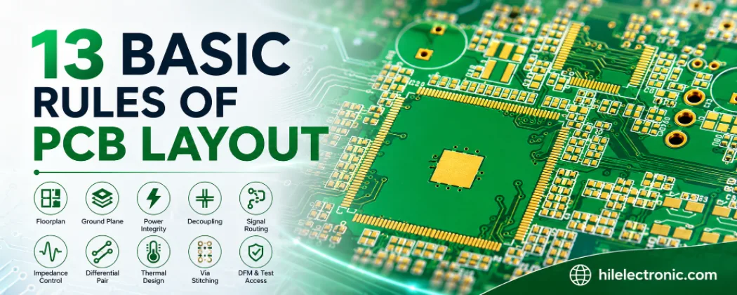
13 Basic Rules of PCB Layout (and the Failures They Prevent)
Figure 1. 13 Basic Rules Of Pcb Layout reference image for...

PCB Current Calculator: Sizing Trace Width and Vias with the IPC-2221 Formula
Figure 1. Pcb Current Calculator reference image for PCB...
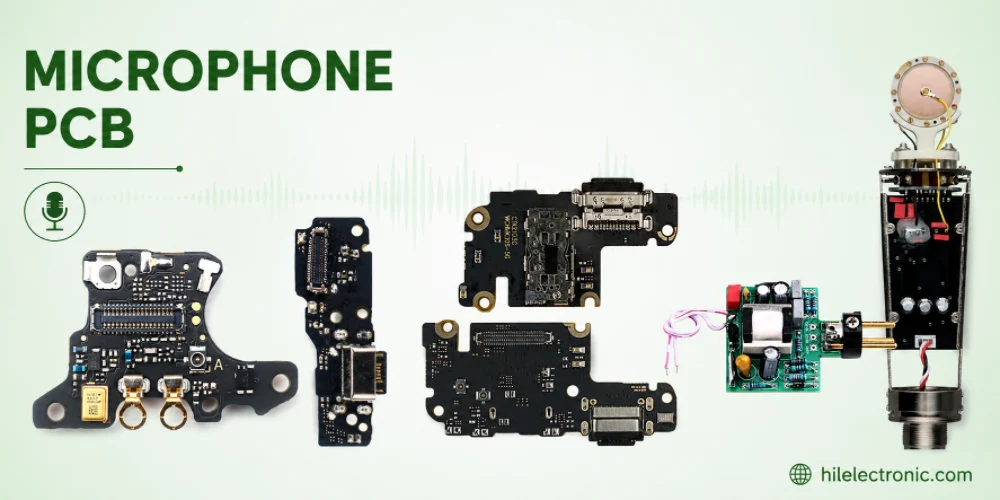
Microphone PCB Design: How the Board Itself Shapes Your Audio Quality
Figure 1. Microphone Pcb reference image for PCB...
How to get a quote for PCBs
Let us run DFM/DFA analysis for you and get back to you with a report.
You can upload your files securely through our website.
We require the following information in order to give you a quote:
-
- Gerber, ODB++, or .pcb, spec.
- BOM list if you require assembly
- Quantity
- Turn time
In addition to PCB manufacturing, we offer a comprehensive range of electronic services, including PCB design, PCBA (Printed Circuit Board Assembly), and turnkey solutions. Whether you need help with prototyping, design verification, component sourcing, or mass production, we provide end-to-end support to ensure your project’s success. For PCBA services, please provide your BOM (Bill of Materials) and any specific assembly instructions. We also offer DFM/DFA analysis to optimize your designs for manufacturability and assembly, ensuring a smooth production process.