
UV LED PCB: Complete Technical Guide for Professional Applications

What is UV LED PCB Technology
UV LED PCB refers to specialized printed circuit boards engineered to drive and support ultraviolet light-emitting diodes across UV-A (315-400nm), UV-B (280-315nm), and UV-C (200-280nm) wavelength ranges. These circuit boards serve as the foundation for UV curing systems, medical phototherapy equipment, sterilization devices, and industrial exposure machines.
Unlike conventional LED PCBs, UV LED printed circuit boards must address higher thermal density, stringent power management requirements, and wavelength stability demands that directly impact application performance and component longevity.
UV LED PCB Structure and Working Principle
Basic Structure Components
A UV LED PCB typically comprises three integrated layers working together to achieve optimal performance. The substrate layer utilizes aluminum-based materials, ceramic substrates, or copper-core constructions selected for superior thermal conductivity properties. The solder mask and reflective layers require UV-resistant formulations to prevent degradation and maintain optical efficiency under continuous ultraviolet exposure.
Working Principle
The working principle involves electrical current flowing through precision-designed copper traces to power LED chips, which convert electrical energy into ultraviolet photons. The UV LED PCB simultaneously manages electrical distribution while conducting waste heat away from the junction, maintaining optimal operating temperatures below 85°C for reliable performance.
Key Design Considerations for UV LED PCBs
Thermal Management Architecture
Thermal management represents the most critical design parameter in UV LED PCB development. Junction temperature directly impacts both light output efficiency and operational lifespan, requiring thermal architectures that incorporate substrate materials with thermal conductivity exceeding 2 W/m·K. Aluminum substrates typically provide 1.5-3 W/m·K, while ceramic options such as aluminum nitride deliver values exceeding 20 W/m·K for high-power applications.
Heat dissipation pathways must minimize thermal resistance at every interface from LED junction through substrate to external heatsinking. Advanced UV LED PCB designs incorporate thermal vias, copper coin technology, or direct bonded copper layers to enhance heat spreading efficiency.
Electrical Layout and Current Distribution
The electrical architecture of UV LED PCBs demands independent driver channels for each LED or LED string to prevent current imbalance. Copper trace thickness typically specifies minimum 2 oz copper weight, with wider traces and shorter routing paths reducing resistive losses. Power supply decoupling and ground plane design minimize return path impedance while maintaining electromagnetic compatibility.
Material Selection for UV Applications
Material selection for UV LED PCBs addresses unique challenges posed by ultraviolet radiation exposure. The solder mask must resist photochemical degradation using specialized UV-resistant formulations that prevent yellowing and mechanical breakdown. Dielectric insulation layers balance thermal conductivity between 2-5 W/m·K against electrical isolation requirements, with thickness ranging from 50 to 150 microns depending on voltage specifications.
Optical and Reflective Layer Design
Reflective layers surrounding UV LEDs must utilize materials with high UV-spectrum reflectivity while demonstrating resistance to discoloration. Silver-white reflective inks formulated specifically for UV applications provide optimal performance. Surface finish selection favors immersion silver or electroless nickel immersion gold over organic solderability preservatives that may degrade under UV exposure.
Reliability and Lifespan Factors
Long-term reliability depends on material stability and thermal stress control. All components should withstand repeated thermal cycling without delamination or solder fatigue. Protective conformal coatings help prevent oxidation and UV-induced degradation. Using RoHS-compliant, high-temperature solders improves joint integrity, while rigorous burn-in and accelerated aging tests validate performance consistency.
By optimizing heat dissipation, electrical uniformity, and UV-resistant materials, designers can significantly extend the operational lifespan of UV LED assemblies and ensure sustained optical output over thousands of hours.

UV LED
Common Types of UV LED PCB Constructions
Aluminum-Based UV LED PCB
Aluminum-based UV LED PCBs represent the most widely deployed solution for moderate to high-power applications including curing lamps and industrial UV printers. These boards combine thermal conductivity ranging from 1.5 to 3 W/m·K with cost-effective manufacturing and good mechanical properties, making them suitable for most commercial UV LED applications.
Ceramic UV LED PCB
Ceramic UV LED PCBs deliver superior performance for demanding medical phototherapy and UV-C sterilization modules requiring exceptional thermal management. Aluminum nitride or aluminum oxide substrates offer thermal conductivity exceeding 20 W/m·K while maintaining excellent electrical insulation and dimensional stability across wide temperature ranges.
Copper-Core UV LED PCB
Copper-core UV LED PCBs serve ultra-high-power exposure equipment where maximum thermal dissipation becomes essential. The copper substrate provides thermal conductivity approaching 400 W/m·K, enabling compact designs for industrial UV curing systems with extreme power density requirements.
Primary Applications of UV LED PCB Technology
UV LED PCBs enable critical applications across multiple industries with distinct performance requirements:
- Medical devices – Phototherapy instruments, dental curing systems, and therapeutic equipment requiring precise wavelength control and biocompatible materials for patient safety.
- Industrial curing systems – UV adhesive polymerization, printing ink curing, and spot-source systems demanding high optical power density and continuous duty cycle reliability.
- Sterilization equipment – UV-C air purification, water treatment devices, and surface disinfection systems leveraging germicidal effectiveness with mercury-free LED technology.
- Exposure and imaging – PCB photoresist exposure, 3D printing light engines, and photolithography equipment requiring wavelength stability and uniform intensity distribution.

UV LED PCBs
UV LED PCBs Manufacturing and Assembly
SMT Process Requirements
Surface mount assembly for UV LED PCBs demands reflow soldering profiles carefully controlled to prevent thermal damage while achieving reliable solder joints. The thermal mass of metal-core substrates requires extended preheat zones with peak temperatures ranging from 240 to 260°C. Lead-free SAC305 alloy represents the standard choice meeting RoHS compliance requirements.
Quality Control and Testing
Assembled UV LED PCBs undergo comprehensive verification including optical power measurement, wavelength verification, and thermal imaging analysis. Automated optical inspection systems check solder joint quality and component placement accuracy, while reliability testing includes thermal cycling and accelerated life procedures customized to application requirements.
Advantages of Professional UV LED PCB Design
Professionally engineered UV LED PCBs deliver measurable performance improvements through optimized thermal architecture and material selection:
- Extended operational lifespan – Reduced junction temperatures through proper thermal design extend LED life by 30-50% compared to generic solutions.
- Stable light output – Precise current management and thermal control maintain consistent intensity over operational life, ensuring reliable process results.
- Optical efficiency – UV-resistant materials prevent degradation and maintain reflectivity across thousands of operating hours.
- Design optimization – Custom LED array configurations and thermal solutions tailored to specific application requirements.
Why Choose Highleap Electronics for UV LED PCBs
Highleap Electronics provides professional UV LED PCB manufacturing and assembly services designed for demanding applications such as curing systems, medical devices, and industrial exposure equipment. Our engineering expertise and precision production ensure high reliability, stable optical performance, and long service life even under continuous ultraviolet irradiation.
Advanced Manufacturing Capabilities
- Material Versatility – Support for aluminum, ceramic (AlN/Al₂O₃), and copper-based UV LED PCBs to meet different thermal and mechanical requirements.
- High-Power Assembly – SMT lines equipped for large-size UV LED packages and multi-channel driver configurations.
- Lead-Free Soldering Process – Full RoHS-compliant manufacturing using high-temperature, UV-stable solder alloys.
- Precision Thermal Control – Integration of copper coin, DBC, and thermal via technologies to enhance heat dissipation efficiency.
Reliability and Quality Assurance
Every UV LED PCB undergoes a comprehensive reliability validation process:
- Thermal cycling and power aging tests for long-term stability.
- UV exposure and reflectivity durability tests to prevent material degradation.
- 100% electrical and optical inspection for uniform brightness and wavelength output.
- Full traceability and compliance with ISO 9001, ISO 14001, and UL standards.
Representative Process Capabilities
| Parameter | Capability Range | Typical Value |
|---|---|---|
| Thermal Conductivity | 1.5 – 20 W/m·K | Aluminum Nitride: 20 W/m·K |
| Copper Thickness | 1 – 4 oz | 2 oz standard |
| SMT Placement Accuracy | ±0.05 mm | ±0.03 mm typical |
| Max Power Density | up to 30 W/cm² | — |
| Surface Finish Options | ENIG, Immersion Silver, HASL | ENIG recommended for UV boards |
Engineering Support
Highleap’s R&D and application teams collaborate closely with clients to customize UV LED PCB solutions, from substrate selection to optical and thermal simulation. We help reduce design cycles and ensure optimal performance for your curing or sterilization systems. Partner with Highleap Electronics to achieve reliable, high-performance UV LED PCB designs engineered for durability, precision, and industrial-grade efficiency.

Recommended Posts
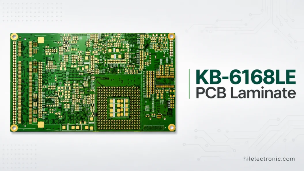
KB-6168LE PCB Laminate for Low Z-CTE Multilayer PCB Manufacturing
KB-6168LE PCB laminate is a Kingboard high-Tg, anti-CAF,...
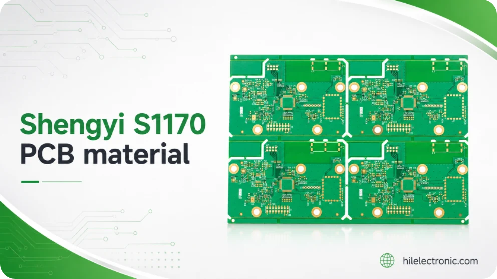
Shengyi S1170 PCB Material for High-Tg Lead-Free Multilayer PCB Manufacturing
Shengyi S1170 PCB material is a lead-free compatible,...

NP-175F PCB Laminate for High-Reliability Multilayer Boards
NP-175F PCB laminate is a Nan Ya high-Tg, filled...

High CTI FR-4 PCB Manufacturing for Insulation-Critical Boards
High CTI FR-4 is used when a PCB design needs stronger...
How to get a quote for PCBs
Let‘s run DFM/DFA analysis for you and get back to you with a report. You can upload your files securely through our website. We require the following information in order to give you a quote:
-
- Gerber, ODB++, or .pcb, spec.
- BOM list if you require assembly
- Quantity
- Turn time
In addition to PCB manufacturing, we offer a comprehensive range of electronic services, including PCB design, PCBA, and turnkey solutions. Whether you need help with prototyping, design verification, component sourcing, or mass production, we provide end-to-end support to ensure your project’s success.
For PCBA services, please provide your BOM (Bill of Materials) and any specific assembly instructions. We also offer DFM/DFA analysis to optimize your designs for manufacturability and assembly, ensuring a smooth production process.