
Back to blog
3D Printing: GPT Innovations in PCB Manufacturing

The integration of 3D printing technology in Printed Circuit Board (PCB) manufacturing represents a significant leap forward in electronics design and production. This innovation offers new possibilities in PCB fabrication, from rapid prototyping to complex designs. Let’s explore how 3D printing is revolutionizing PCB manufacturing.
What is 3D printing technology
3D printing technology, also known as additive manufacturing, involves creating three-dimensional objects from a digital file by layering material. This process builds objects layer by layer, using materials like plastic, resin, metal, or even living cells. It enables the creation of complex and customized shapes that might be challenging or impossible to produce with traditional manufacturing methods. 3D printing is widely used in industries such as aerospace, automotive, healthcare, and consumer products for prototyping, tooling, and even final product creation. It offers benefits like reduced waste, design flexibility, and the potential for on-demand production.
What are 3D print Circuit Boards
3D printing of PCBs refers to the process of creating PCBs using additive manufacturing technology. This technique involves layering conductive and insulating materials to form electronic circuits in a three-dimensional space. Unlike traditional PCB manufacturing, which is largely subtractive and involves removing excess material, 3D printing builds the PCB layer by layer from the ground up. This method allows for more design flexibility, can reduce waste, and is particularly useful for rapid prototyping, creating complex or customized circuit layouts, and integrating electronic components into unique form factors.
Advantage of 3D printing PCB
- Rapid Prototyping: Allows for quick creation and testing of PCB designs.
- Complex Designs: Enables the manufacturing of PCBs with intricate and non-standard shapes.
- Reduced Waste: Additive manufacturing minimizes material wastage compared to traditional subtractive methods.
- Integrated Components: Possibility to integrate components directly into the PCB during the printing process.
- Cost-Effective for Small Batches: More economical for producing small quantities or custom designs.
- Design Flexibility: Facilitates easy modifications and iterations in design.
Innovations in 3D Printing for PCBs
- Advanced Conductive Inks:Development in nanoparticle-infused inks that offer better conductivity and adherence to various substrates.Experimentation with graphene and other novel materials for enhanced electrical properties.
- Multi-Material 3D Printing:Printers capable of handling both conductive and insulating materials simultaneously, enabling the production of entire PCBs in a single print cycle.
Integration of flexible and rigid materials within the same PCB for innovative applications. - High-Precision 3D Printers:Enhanced resolution and precision in 3D printers, allowing for finer trace widths and spacing, suitable for complex circuit designs.Improved layer adhesion techniques to ensure structural integrity and reliability.
Emerging Trends in 3D Printed PCBs
- Printed Electronics and IoT Devices:Utilization in IoT and wearable devices, where flexibility and form factor are critical.Development of 3D printed sensors and antennas integrated into PCBs.
- Rapid Prototyping and Customization:Facilitation of quick iterations in design, crucial for R&D and bespoke electronics.On-demand manufacturing capabilities for personalized electronics and small-run productions.
- Sustainability and Material Innovation:Exploration of eco-friendly and recyclable materials for PCB printing.Research on reducing energy consumption and waste in the PCB manufacturing process.
Challenges and Limitations of 3D printing PCBs
- Limited Material Options: The range of materials suitable for 3D printing PCBs is currently limited compared to traditional methods.
- Lower Conductivity: Materials used in 3D printed PCBs may have lower electrical conductivity than those used in conventional PCBs.
- Durability Concerns: 3D printed PCBs might not be as durable or reliable for long-term use or in harsh environments.
- Precision and Resolution: Achieving the high precision and resolution required for some PCB applications can be challenging.
- Cost and Speed for Large Scale Production: While cost-effective for small runs, 3D printing can be less economical and slower for mass production.
- Technical Expertise: Designing and printing PCBs using 3D technology requires specialized knowledge and skills.
Conclusion
The intersection of 3D printing technology with PCB manufacturing is fostering a new era of technological innovations and trends. From advanced conductive materials to hybrid manufacturing techniques, these advancements are not only enhancing
the capabilities of PCB production but also opening doors to new applications and efficiencies. As research and development continue, the future of 3D printed PCBs looks promising, potentially transforming the electronics manufacturing landscape with more sustainable, flexible, and customized solutions. The key will be harnessing these innovations to overcome current limitations, paving the way for broader adoption and novel applications in various sectors of the electronics industry.
When the project moves from research to an RFQ, review PCB layout review and PCB finish selection so the material, process, and inspection requirements stay aligned.

Related Articles
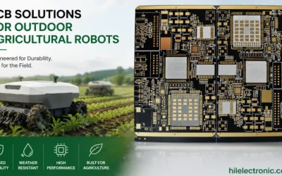
Outdoor Agricultural Robot PCB for Rugged Field Electronics
Outdoor agricultural robot PCB manufacturing for rugged field electronics, coatings, connectors, power protection, EMC control, and assembly.
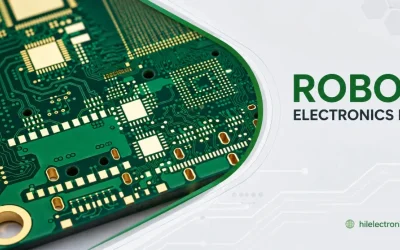
Robot Electronics PCB Design and Manufacturing for Reliable Robotics
Robot electronics PCB design and manufacturing guidance for control, power, sensor, vision, and motor-drive boards.
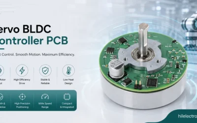
Servo and BLDC Controller PCB Design and Manufacturing
Servo and BLDC controller PCB guidance for FOC, encoder feedback, current sensing, EtherCAT, and calibration.