
Our PCB Assembly Process–Highleap Electronic

The PCB assembly process transforms a fabricated bare board into a functional electronic product by mounting components, soldering connections, inspecting quality, and verifying electrical performance. For OEMs, hardware startups, engineers, and procurement teams, understanding this process is important not only for product quality, but also for lead time, manufacturability, and cost control.
At Highleap Electronics, we provide PCB assembly services for prototype, low-volume, and mass production projects across consumer, industrial, automotive, communication, and medical applications. This guide explains the complete PCB assembly process step by step, from design file review and component sourcing to SMT placement, soldering, inspection, testing, and final delivery.
Table of Contents
- What Is PCB Assembly?
- Step 1: File Review and Engineering Preparation
- Step 2: Component Sourcing and Incoming Inspection
- Step 3: Solder Paste Printing and SPI
- Step 4: SMT Component Placement
- Step 5: Reflow Soldering
- Step 6: Through-Hole Assembly and Secondary Soldering
- Step 7: Inspection and Testing
- Step 8: Final Assembly, Cleaning, and Shipment
- What Files We Need for PCB Assembly
- PCB Assembly Process FAQ
What Is PCB Assembly?
PCB assembly, often abbreviated as PCBA, is the process of mounting and soldering electronic components onto a printed circuit board so that the board becomes electrically functional. A bare PCB contains copper traces, pads, solder mask, and drilled holes, but it cannot perform its intended function until components such as resistors, capacitors, ICs, connectors, switches, and other devices are assembled onto it.
The PCB assembly process can include both surface-mount technology (SMT) and through-hole technology (THT), depending on the design. In modern electronics manufacturing, SMT is used for most components because it supports high-speed, high-density, and automated assembly. Through-hole assembly is still common for connectors, transformers, relays, terminal blocks, large capacitors, and mechanically stressed parts.
Step 1: File Review and Engineering Preparation
The PCB assembly process starts before any component enters the production line. The first stage is engineering preparation, where the design package is reviewed for completeness, manufacturability, and assembly readiness.
Typical files checked at this stage include:
- Gerber files
- BOM (bill of materials)
- Pick-and-place file or centroid data
- Assembly drawings
- Special process notes
- Programming or test requirements if applicable
This step is critical because many production issues are caused by incomplete BOM information, incorrect footprints, polarity ambiguity, mismatched package definitions, or missing assembly instructions. Early review helps avoid delays, rework, and costly production mistakes.
Step 2: Component Sourcing and Incoming Inspection
After the design package is confirmed, components are sourced according to the BOM. Depending on the project, this may involve turnkey assembly with full procurement, consigned assembly with customer-supplied parts, or a mixed sourcing model.
Before assembly begins, incoming materials are checked to verify:
- Correct part numbers and package types
- Quantity and lot consistency
- Packaging condition and reel suitability for SMT use
- Moisture-sensitive device status where applicable
- Date code and traceability requirements if needed
Good incoming inspection reduces the risk of wrong-part loading, feeder errors, soldering issues, and reliability problems later in the process.
Step 3: Solder Paste Printing and SPI
For SMT assemblies, solder paste printing is one of the most important steps in the entire PCB assembly process. Solder paste is applied to PCB pads through a stencil so that components can later be mounted and soldered during reflow.
Printing quality depends on several factors:
- Correct stencil thickness and aperture design
- Accurate alignment using fiducials
- Stable squeegee pressure and print speed
- Proper solder paste condition and viscosity
After printing, many production lines use solder paste inspection (SPI) to check paste volume, height, area, and alignment. This helps catch defects early before they become placement or soldering failures.
Step 4: SMT Component Placement
Once solder paste has been applied, SMT components are placed on the PCB using automated pick-and-place machines. This stage turns digital placement data into real assembly on the board.
Placement accuracy depends on:
- Machine calibration
- Correct feeder setup
- Reliable vision alignment
- Proper nozzle selection
- Accurate component recognition
Fine-pitch ICs, QFNs, BGAs, and very small passive components such as 0201 or 01005 devices require especially tight control. Even small placement offsets can cause bridging, opens, or hidden solder defects after reflow.
Step 5: Reflow Soldering
After SMT placement, the board passes through a reflow oven, where the solder paste melts and forms permanent solder joints between the components and the PCB pads. This is one of the most critical stages because it directly determines solder joint integrity for most surface-mounted parts.
A controlled reflow profile includes:
- Preheat
- Soak
- Time above liquidus
- Peak temperature
- Controlled cooling
If the thermal profile is poorly managed, defects such as tombstoning, insufficient wetting, solder balls, voiding, cold joints, or thermal stress can occur. For advanced assemblies, nitrogen reflow may be used to reduce oxidation and improve soldering consistency.
Step 6: Through-Hole Assembly and Secondary Soldering
Many PCB assemblies include both SMT and through-hole components. Through-hole assembly is commonly used for connectors, power components, relays, terminal blocks, transformers, and parts that need stronger mechanical support.
These components may be soldered by:
- Wave soldering
- Selective soldering
- Manual soldering
The correct method depends on the board design, thermal sensitivity, component mix, and production volume. Selective soldering is particularly useful for mixed-technology boards where local control is needed without disturbing nearby SMT parts.
Step 7: Inspection and Testing
Inspection and testing ensure that the assembled PCB meets both visual and electrical requirements before shipment. A reliable PCB assembly process does not end at soldering. It includes systematic verification.
Common inspection and test methods include:
- AOI (Automated Optical Inspection): checks for missing parts, polarity errors, misalignment, bridging, and visible defects
- X-ray inspection: used for BGAs, QFNs, hidden joints, and void analysis
- ICT (In-Circuit Testing): checks electrical connectivity and component-level faults
- Functional testing: confirms that the board operates correctly in its intended working state
- Burn-in or aging tests: used for critical or high-reliability products
The inspection strategy depends on product complexity, reliability requirements, application risk, and cost target. For industrial, medical, and communication products, test coverage is often a major part of outgoing quality control.
Step 8: Final Assembly, Cleaning, and Shipment
After inspection and testing, the PCB assembly may go through final steps such as cleaning, conformal coating, mechanical installation, label application, anti-static packaging, moisture barrier packing, or customer-specific shipment preparation.
This final stage matters because handling, packaging, and labeling affect whether the boards arrive ready for use, especially in export, industrial, and high-mix manufacturing environments.
What Files We Need for PCB Assembly
To quote and prepare a PCB assembly project accurately, the manufacturer typically needs more than just the bare PCB files. A complete package improves quotation accuracy and makes engineering review more useful.
The recommended file set includes:
- Gerber files
- BOM with manufacturer part numbers
- Pick-and-place or centroid data
- Assembly drawing
- Special process notes
- Programming or test instructions if required
- Quantity and lead time requirements
The more complete the data package, the easier it is to avoid engineering confusion, sourcing delays, and assembly preparation errors.
PCB Assembly Process FAQ
What is the difference between PCB fabrication and PCB assembly?
PCB fabrication produces the bare board, including copper layers, drilled holes, solder mask, and surface finish. PCB assembly mounts and solders components onto that board so it becomes electrically functional.
Is PCB assembly only SMT?
No. Many assemblies use both SMT and through-hole technology. The correct process depends on the component mix and mechanical or electrical requirements of the product.
Why is solder paste printing so important?
Solder paste printing affects the quality of nearly all SMT solder joints. Poor paste volume or alignment can lead to bridging, opens, tombstoning, or weak joints later in the process.
Why is testing important in PCB assembly?
Testing helps detect visual defects, electrical faults, hidden soldering problems, and functional failures before the boards are shipped or installed in products.
What is needed before starting PCB assembly?
A complete design package is needed, including Gerber files, BOM, pick-and-place data, assembly drawings, and any special process or test requirements.
Can the same PCB assembly process support both prototype and mass production?
Yes. The overall process structure is similar, but machine setup, inspection depth, test strategy, and efficiency targets may differ depending on the build quantity and product complexity.
Engineers usually confirm this topic together with Gerber and drill package and immersion gold surface finish when preparing a reliable PCB or PCBA build.

Related Articles
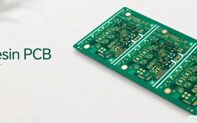
BT Resin PCB: Properties, Uses, and Fabrication Controls
Learn what a BT resin PCB is, how BT compares with FR-4, and why the laminate is used for BGA substrates and high-reliability packages.
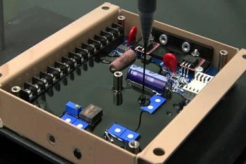
PCB Potting Services: Compounds, Process, and Design Rules
Learn when PCB potting services make sense, compare epoxy, polyurethane, and silicone, and design assemblies for sealed protection.
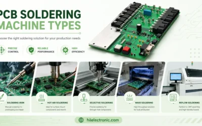
PCB Soldering Machine Types: Reflow, Wave, and Selective Equipment
Compare PCB soldering machine types, from reflow ovens to wave and selective systems, and match the right equipment to your assembly mix.