
Cost-Optimized Edge Computing PCB Design

As edge computing transforms the way data is processed by moving computational power closer to data sources, it has become a pivotal technology in industries ranging from industrial IoT to autonomous vehicles and smart cities. The global edge computing market is poised to reach $87 billion by 2025, and the demand for high-performance, reliable PCB solutions that support these distributed systems is skyrocketing. At Highleap Electronics, we specialize in providing advanced PCB manufacturing services that address the unique challenges of edge computing, offering unparalleled expertise in miniaturization, thermal management, and reliability.
Understanding Edge Computing PCB Requirements
Edge computing devices must operate efficiently in a variety of challenging environments—from factory floors housing industrial IoT sensors to autonomous vehicle systems and urban smart city infrastructures. These applications require PCBs that not only handle demanding processing tasks but also meet stringent space, performance, and reliability requirements.
The key challenge in designing edge computing PCBs is balancing high computational power with the need for compact form factors and minimal cooling. Unlike traditional data center boards, which benefit from larger footprints and active cooling, edge PCBs must deliver exceptional performance within small spaces while managing heat passively or with minimal cooling solutions. To meet these challenges, many edge computing designs leverage HDI PCB technology to achieve high-density interconnections in a compact footprint.
Signal integrity is paramount in edge computing, as modern applications require data transmission speeds exceeding 25 Gbps. High-speed processing and densely packed components demand precise impedance control, advanced stackup design, and the use of high-quality materials to minimize signal loss and interference. By selecting the right PCB assembly process , these issues can be effectively managed, ensuring reliable operation in demanding environments.
Critical Design Considerations for Edge Computing PCBs
High-Density Interconnect (HDI) Technology
Edge computing applications require high-density interconnect (HDI) technology to achieve high component density in small, space-constrained designs. At Highleap Electronics, we utilize micro-vias as small as 0.05mm, enabling intricate routing within compact layouts. Our advanced HDI processes, such as sequential lamination, allow for multi-layered interconnections that support powerful processors and AI accelerators, ensuring low latency and optimal signal integrity.
By optimizing impedance control, precise stackup design, and high-speed signal routing, we guarantee that your edge computing PCBs meet stringent performance requirements in even the smallest form factors.
Balancing Component Limitations with Design Constraints
In edge computing, component limitations go beyond just size; there are also market, policy, and cost constraints that influence PCB design decisions.
- Market Constraints: Certain components may face limited availability due to supply chain fluctuations or shifts in the market. This can limit your choice of parts, requiring flexible design adjustments to accommodate available components without sacrificing performance.
- Policy Constraints: Depending on the application, there may be regulatory requirements or industry-specific standards (e.g., automotive, medical, or aerospace) that restrict certain materials, design features, or manufacturing processes. For example, compliance with RoHS (Restriction of Hazardous Substances) may require substitution of certain materials, affecting both the design and cost.
- Cost Constraints: Edge computing devices often need to strike a balance between performance and cost. High-performance components, such as advanced processors or AI chips, can quickly drive up the cost of the PCB. At Highleap Electronics, we optimize the layer count and material selection to reduce costs, while still meeting functional and performance requirements.
By leveraging HDI technology, we minimize the number of layers required for routing, supporting complex designs without exceeding size or budget constraints. Additionally, we carefully select materials that provide the best performance at a cost-effective price point, ensuring your project remains financially viable while still achieving optimal results.
Material Selection for Harsh Environments
Edge computing devices are often deployed in environments subject to extreme temperatures, humidity, vibration, and electromagnetic interference (EMI). The selection of materials is crucial to ensuring the PCB’s reliability and performance under such conditions.
At Highleap Electronics, we offer a range of materials tailored to meet the demands of edge computing applications. For high-frequency applications, we use low-loss materials like Rogers RO4000 and Isola I-Tera MT40, which provide stable electrical properties even across wide temperature ranges. These materials help maintain signal integrity and ensure that your design performs reliably over time. For more information on suitable materials, check out our PCB Laminate Material guide, or feel free to reach out to us directly with any questions.
For applications requiring enhanced thermal management, we use thermally conductive substrates that help reduce junction temperatures by up to 30%. To protect sensitive components from moisture, dust, and chemicals, we also offer conformal coating and potting services, ensuring durability in harsh environments.

Cost-Effective Strategies for Manufacturing Edge Computing PCBs
1. Optimize Layer Count
Reducing the number of layers in your edge computing PCB design can significantly lower manufacturing costs. While HDI technology is ideal for compact, high-performance designs, unnecessary layers increase both material and fabrication complexity.
By collaborating with your manufacturer, you can assess whether additional layers are essential for performance and explore opportunities to consolidate layers, optimizing costs without compromising functionality. This approach is especially relevant for designs like GPU PCBs or high-performance computing PCBs.
2. Use Materials Efficiently
The choice of materials directly impacts PCB costs. High-performance materials like low-loss substrates or thermally conductive materials are necessary in some areas, but many designs can benefit from more affordable alternatives for non-critical components.
Evaluate material requirements early on to avoid over-specifying. By selecting cost-effective options for non-essential areas, you can maintain PCB integrity while reducing material costs. For example, in AI computing hardware PCB manufacturing, balancing material selection can achieve high performance without unnecessarily inflating costs.
3. Apply Design for Manufacturing (DFM)
Integrating Design for Manufacturing (DFM) principles ensures that your design is optimized for production, reducing complexity and manufacturing costs. Simplifying vias and ensuring proper component spacing can prevent costly redesigns and delays, especially in server PCBs where density and efficiency are crucial.
Engage your manufacturer early for DFM reviews to identify potential challenges like tight component placements or routing difficulties. These adjustments made before production starts can ultimately save both time and money, ensuring smooth manufacturing processes for your edge computing or AI computing hardware PCB manufacturing needs.
4. Streamline Testing
Testing is vital, but over-testing can add unnecessary costs. Focus your testing efforts on critical areas such as signal integrity and thermal management that directly affect performance, particularly in high-performance applications like GPU PCBs and server PCBs.
By prioritizing essential tests and avoiding redundant ones, you can minimize testing costs while ensuring the PCB meets all functional requirements, making the process more cost-effective.
5. Simplify Assembly
Efficient assembly plays a key role in reducing overall production costs. Opting for mixed-technology assembly, which integrates SMT and through-hole components, minimizes the need for multiple assembly steps, reducing labor costs and time.
Designing with automation in mind also speeds up the process. Working closely with your assembly team ensures that the PCB is easy to assemble, cutting down on delays and manual labor. For complex designs like AI computing hardware PCBs, this strategy is crucial for reducing assembly time and cost.
6. Manage Component Sourcing
Component availability can affect both cost and production schedules, especially when supply chain issues arise. To avoid delays and rising prices, opt for readily available components that meet your design’s requirements.
Maintain flexibility by sourcing alternative components that are more cost-effective and easier to acquire. Collaborating with your manufacturer can help identify reliable alternatives, ensuring smooth production and predictable costs, especially for server PCBs and high-performance computing PCBs where sourcing specific components can be challenging.
Partner with Highleap Electronics
For successful edge computing deployments, cost-optimized edge computing PCB design is essential. Choosing the right partner means balancing performance, reliability, and total cost of ownership. At Highleap Electronics, we integrate advanced manufacturing technology with proven expertise in edge computing applications to deliver PCBs tailored to your exact needs.
From early design consultation to rapid prototyping, volume production, and lifecycle quality assurance, we provide end-to-end support that ensures efficiency and scalability. Our engineering team specializes in creating PCB solutions that meet demanding technical requirements while controlling costs, helping you bring innovative products to market faster.
Transform your edge computing vision into reality with Highleap Electronics’ manufacturing capabilities. Get Started Today — request a quote or schedule a consultation, and discover how our expertise in cost-optimized edge computing PCB design can accelerate your next project.

Related Articles
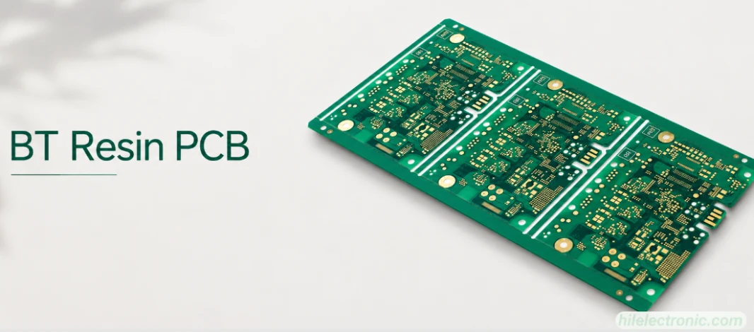
BT Resin PCB: Properties, Uses, and Fabrication Controls
Figure 1. BT resin PCB image for PCB manufacturing...
PCB Potting Services: Compounds, Process, and Design Rules
Figure 1. PCB potting services image for Highleap...
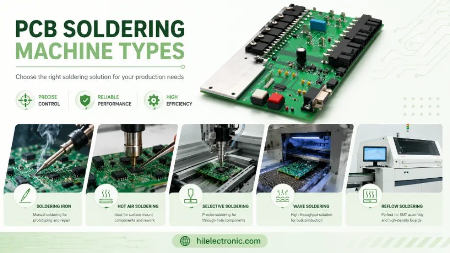
PCB Soldering Machine Types: Reflow, Wave, and Selective Equipment
Figure 1. PCB soldering machine types image for Highleap...

Clean Flux vs No-Clean Flux: Residue, Cleaning, and PCB Reliability
Figure 1. clean flux vs no-clean flux image for Highleap...
How to get a quote for PCBs
Let us run DFM/DFA analysis for you and get back to you with a report.
You can upload your files securely through our website.
We require the following information in order to give you a quote:
-
- Gerber, ODB++, or .pcb, spec.
- BOM list if you require assembly
- Quantity
- Turn time
In addition to PCB manufacturing, we offer a comprehensive range of electronic services, including PCB design, PCBA (Printed Circuit Board Assembly), and turnkey solutions. Whether you need help with prototyping, design verification, component sourcing, or mass production, we provide end-to-end support to ensure your project’s success. For PCBA services, please provide your BOM (Bill of Materials) and any specific assembly instructions. We also offer DFM/DFA analysis to optimize your designs for manufacturability and assembly, ensuring a smooth production process.