
MCPCB Dielectric Layer: How to Balance Thermal Conductivity and Electrical Insulation

Introduction to MCPCB Dielectric Layer Design
Metal Core Printed Circuit Boards have become indispensable in high-power applications spanning LED lighting systems, power conversion modules, and automotive electronics where thermal management directly impacts device reliability. The MCPCB dielectric layer serves as the critical interface between circuit traces and the metal substrate, simultaneously providing electrical insulation while facilitating efficient heat transfer from components to the base plate.
This dual functionality makes dielectric layer design one of the most crucial factors determining overall board performance in thermal-intensive applications. The challenge lies in balancing competing requirements: thinner layers improve thermal conductivity but compromise dielectric strength, while material selection affects both manufacturing feasibility and long-term reliability.
Understanding how to optimize MCPCB dielectric layer thickness and material properties enables engineers to design boards that meet specific thermal and electrical requirements without over-engineering or introducing unnecessary cost.
Core Functions of the MCPCB Dielectric Layer
Thermal Performance Management
The dielectric layer functions as the primary thermal interface conducting heat from copper circuitry to the aluminum or copper base plate. Thermal resistance through this layer follows the equation R = t/(k·A), where t represents thickness, k denotes thermal conductivity, and A indicates cross-sectional area.
This relationship reveals why even minor variations in MCPCB dielectric layer thickness or material selection significantly impact junction temperatures in high-power components. In LED applications operating at 3-5 W/cm² heat flux density, reducing dielectric thermal resistance by 0.5 °C·cm²/W can lower junction temperatures by 15-25°C, directly extending operational lifetime.
Electrical Isolation Requirements
Beyond thermal management, the dielectric layer must maintain electrical integrity under operating voltages while preventing breakdown or tracking between circuit traces and the grounded metal substrate. Dielectric strength typically ranges from 2-4 kV for standard polyimide materials to over 10 kV for specialized ceramic-filled composites.
Applications involving high voltage or harsh environmental conditions require careful material selection to ensure adequate safety margins. The insulation material must also maintain stable dielectric properties across the operating temperature range, which in automotive or industrial applications may span from -40°C to +150°C.

Metal Core PCB Stackup
Dielectric Material Selection for MCPCB
Common Material Systems
The selection of appropriate insulation materials fundamentally determines MCPCB dielectric layer performance characteristics. Three primary material categories dominate modern metal core board manufacturing:
- Standard Polyimide-Based Dielectrics – Offer thermal conductivity of 0.2-0.5 W/mK with excellent processing compatibility for conventional PCB lamination equipment, providing adequate performance for moderate power applications while maintaining cost-effectiveness and manufacturing scalability.
- Enhanced Polymer Formulations – Incorporate ceramic fillers to achieve 1-3 W/mK thermal conductivity, bridging the gap between basic polymers and full ceramic systems while maintaining reasonable processing compatibility and cost structure.
- Advanced Ceramic Composites – Materials including aluminum nitride (AlN) and silicon nitride (Si₃N₄) based dielectrics deliver thermal conductivity from 3-8 W/mK, approaching the performance of direct bonded copper on ceramic substrates for extreme heat flux applications.
Material Selection Criteria
Material selection for the MCPCB dielectric layer requires balancing thermal conductivity against dielectric strength, processing compatibility, and cost constraints. High thermal conductivity materials naturally reduce thermal resistance but may exhibit lower dielectric strength per unit thickness, necessitating thicker layers that partially offset thermal gains.
The optimal material depends on specific heat flux requirements, operating voltages, environmental conditions, and production volume economics. Manufacturing compatibility extends beyond initial lamination to include considerations for drilling, routing, surface finishing, and assembly processes that may stress the dielectric layer.
MCPCB Dielectric Layer Thickness Control
Impact on Thermal and Electrical Performance
Dielectric thickness directly governs the thermal resistance between circuit layer and metal base, with typical ranges from 50-200 μm depending on application requirements. Reducing thickness from 100 μm to 75 μm in a 2 W/mK material decreases thermal resistance by 25%, corresponding to significant junction temperature reduction in high-power designs.
However, diminishing returns occur as thickness approaches manufacturing capability limits. Electrical considerations constrain minimum thickness based on required breakdown voltage and safety factors.
A 100 μm MCPCB dielectric layer with 3 kV/mm dielectric strength provides 300V breakdown capacity, adequate for most LED and moderate power applications. High voltage designs may mandate 150-200 μm thickness even where thermal performance would benefit from thinner construction.
Optimization Methods
Optimal MCPCB dielectric layer thickness emerges from thermal modeling that incorporates actual power dissipation, component layout, and ambient conditions against electrical requirements defined by operating voltages and safety standards. Manufacturing capability establishes the practical lower bound, typically 50-75 μm for volume production processes.
Upper limits around 200-250 μm maintain acceptable thermal performance while providing sufficient dielectric strength. Thickness uniformity across the panel affects both thermal and electrical consistency, with manufacturing controls targeting ±10% thickness variation to ensure predictable performance.
Advanced lamination processes using calibrated prepreg systems achieve tighter tolerances when application requirements justify additional process control. Critical factors for thickness optimization include:
- Thermal Requirements – Calculate maximum allowable thermal resistance based on component power dissipation and target junction temperatures, then determine thickness limits for selected dielectric material.
- Electrical Safety Margins – Establish minimum thickness based on peak operating voltage multiplied by appropriate safety factors (typically 2-3x) and material dielectric strength rating.
- Manufacturing Tolerances – Account for practical fabrication variations in lamination processes, ensuring specification windows accommodate normal production variability without compromising performance.

MCPCB Heat Dissipation
Manufacturing Considerations for MCPCB Dielectric Layers
Lamination and Processing
Prepreg-based dielectric layers utilize standard PCB lamination processes adapted for metal substrates, requiring modified pressure and temperature profiles to accommodate different thermal expansion characteristics. The metal core acts as a significant heat sink during lamination, necessitating longer heat-up times and precise temperature control to achieve proper resin flow and adhesion.
Incomplete cure or inadequate bonding compromises both thermal transfer and electrical integrity of the MCPCB dielectric layer. Coefficient of thermal expansion (CTE) mismatch between dielectric layer, copper circuitry, and metal substrate generates mechanical stress during thermal cycling.
Proper material selection ensures CTE compatibility within acceptable limits, typically targeting dielectric CTE within 5-10 ppm/°C of the base metal to minimize stress-induced failures over operational lifetime.
Quality Control and Testing
Ensuring consistent MCPCB dielectric layer performance requires comprehensive testing protocols throughout manufacturing:
- Dielectric Strength Testing – High-pot testing at voltages substantially above rated operation, typically 2-3x operating voltage for production screening, validates electrical integrity and identifies potential defects before assembly.
- Thermal Resistance Measurement – Thermal impedance test equipment confirms heat transfer performance, identifying process variations or material inconsistencies that could compromise thermal management in the final application.
- Microsection Analysis – Destructive testing on representative samples verifies dielectric thickness, void content, and interfacial bonding quality for process qualification and ongoing quality monitoring throughout production runs.
Conclusion: Optimizing MCPCB Dielectric Layer Performance
Effective MCPCB dielectric layer design requires a systematic approach that balances thermal performance, electrical insulation, material properties, and manufacturing constraints. The dielectric layer is the key thermal bottleneck in metal core PCBs, and its optimization is essential to achieve target component temperatures, system reliability, and device longevity. Considerations such as material selection, thickness control, CTE matching, and lamination process integrity are critical for ensuring consistent performance.
Highleap Electronics Capabilities:
-
Precise Material Selection – We help clients choose dielectric materials with optimal thermal conductivity and dielectric strength.
-
Thickness Optimization – Our processes ensure dielectric layers meet both thermal and electrical requirements within manufacturing tolerances.
-
Process Control & Quality Assurance – Attention to lamination, CTE matching, and verification tests guarantees reliable board performance.
-
Integrated System Approach – We consider dielectric layer performance in the context of overall PCB layout, component selection, and thermal architecture.

Recommended Posts
PCB Trace Resistance Calculator: How to Calculate Trace Resistance and Voltage Drop
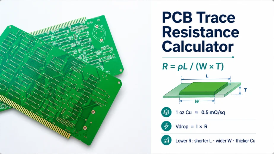
Figure 1. PCB trace resistance affects voltage drop, heat...
PCB Trace Current Capacity: Width, Copper Weight, and IPC-2221
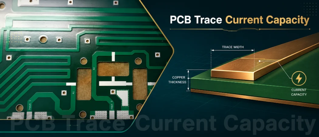
Figure 1. PCB trace current capacity depends on copper...
EAGLE PCB Software: Is It Free, EAGLE vs KiCad, and How to Export Gerber Files
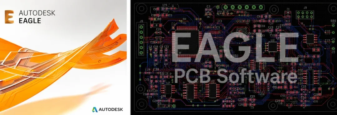
Figure 1. EAGLE PCB software projects should be exported...
Microcontroller Board Soldering and Programming: QFN Pads, SWD, and FTDI Drivers
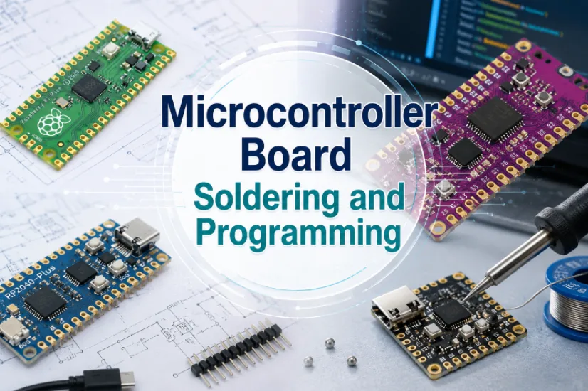
Figure 1. Microcontroller board soldering and programming...
How to get a quote for PCBs
Let‘s run DFM/DFA analysis for you and get back to you with a report. You can upload your files securely through our website. We require the following information in order to give you a quote:
-
- Gerber, ODB++, or .pcb, spec.
- BOM list if you require assembly
- Quantity
- Turn time
In addition to PCB manufacturing, we offer a comprehensive range of electronic services, including PCB design, PCBA, and turnkey solutions. Whether you need help with prototyping, design verification, component sourcing, or mass production, we provide end-to-end support to ensure your project’s success.
For PCBA services, please provide your BOM (Bill of Materials) and any specific assembly instructions. We also offer DFM/DFA analysis to optimize your designs for manufacturability and assembly, ensuring a smooth production process.