
Common MCPCB Design Errors and How to Avoid Them

Understanding the Impact of MCPCB Design Errors
Metal Core Printed Circuit Boards serve critical functions in high-power LED lighting, power conversion modules, and automotive electronics where thermal management determines product longevity. Design errors in MCPCBs typically manifest as thermal failures, signal integrity issues, and premature device degradation that compromise system reliability.
Avoiding MCPCB design errors requires systematic attention to thermal pathways, electrical isolation, and manufacturing constraints throughout the development cycle. Engineers who treat thermal design as an afterthought face the highest risk of costly redesigns and field failures.
Thermal Management Design Errors in MCPCBs
Underestimating Heat Dissipation Requirements
The most prevalent MCPCB design errors stem from inadequate thermal analysis during the conceptual phase. Engineers frequently underestimate actual heat loads by failing to account for ambient temperature variations, duty cycle patterns, and cumulative thermal effects from adjacent components.
Critical factors often overlooked in thermal calculations include:
- Interface thermal resistance – Thermal interface materials add 0.5 to 2°C/W between MCPCB and heat sink, significantly impacting total thermal impedance.
- Ambient condition variations – Temperature derating requirements reduce actual power capacity by 20-40% compared to ideal laboratory conditions.
- Cumulative heat effects – Multiple heat sources create compounding thermal loads that exceed individual component calculations.
Thermal resistance calculations must incorporate the complete heat transfer path from junction to ambient. Simulation tools such as ANSYS or ThermalCAD provide predictive analysis when supplied with accurate material properties and boundary conditions.
Dielectric Layer Selection Mistakes
Selecting dielectric materials based solely on cost considerations represents a fundamental MCPCB design error with severe thermal consequences. The dielectric layer governs overall thermal resistance, with typical thermal conductivity values ranging from 1 to 3 W/m·K for standard materials and up to 5 W/m·K for premium options.
Dielectric thickness selection involves balancing electrical isolation requirements against thermal performance objectives. Thickness ranges from 50 to 150 micrometers, with thinner layers offering lower thermal resistance but reduced dielectric strength. Engineers must evaluate voltage stress levels to prevent breakdown while maintaining acceptable thermal impedance.
Component Layout and Placement Design Errors
Poor Component Distribution Strategies
Component placement errors create localized hot spots that exceed the heat spreading capacity of the metal core substrate. Concentrating high-power devices in small areas generates thermal gradients that cause uneven expansion, leading to delamination between copper foil and dielectric layers.
Effective thermal management requires distributing heat sources across the board area while maintaining logical power delivery paths. Strategic placement of thermal vias in copper regions surrounding power devices enhances lateral heat spreading before transfer through the dielectric layer.
Copper Trace and Pad Design Mistakes
Insufficient copper weight or trace width represents a common MCPCB design error affecting both current carrying capacity and thermal performance. Traces must handle electrical current without excessive resistive heating while also serving as thermal conductors from components to the metal core.
Pad geometry directly influences solder joint thermal and mechanical integrity in MCPCB assemblies. Oversized pads without thermal relief patterns extract excessive heat during soldering, resulting in cold joints. Conversely, undersized pads compromise mechanical strength and thermal coupling to the underlying metal core.

Electrical Isolation Design Errors in High-Voltage MCPCBs
Insufficient Creepage and Clearance Distances
High-voltage MCPCB applications require rigorous attention to electrical spacing requirements that novice designers frequently overlook. Creepage distance, measured along the surface between conductors at different potentials, must meet standards such as IEC 60664 to prevent surface tracking and eventual dielectric failure.
Key electrical spacing requirements include:
- Creepage distance standards – Minimum 0.25 millimeters per kilovolt serves as baseline, adjusted for pollution degree and altitude.
- Clearance through air – Adequate spacing prevents arcing and corona discharge, particularly near conductive metal base plane.
- Solder mask barriers – Additional insulation layers may be required to achieve voltage ratings in compact layouts.
Design errors in electrical spacing often occur when engineers apply standard PCB rules without accounting for the conductive metal base plane proximity. Enhanced insulation coordination may require conformal coating application to achieve required voltage ratings.
Metal Core Grounding Design Errors
Treating the metal core layer as an electrical ground without proper isolation strategy constitutes a significant MCPCB design error in many applications. While the metal base can serve as ground reference in some designs, unintended ground loops and noise coupling occur when multiple ground points create circular current paths.
Systems requiring electrical isolation between the metal core and circuit ground need particular attention during layout and assembly. Design documentation must clearly communicate isolation requirements to prevent assembly errors that compromise safety.
Manufacturing and Assembly Design Errors
Ignoring Design for Manufacturability Principles
MCPCB design errors frequently emerge from lack of communication with manufacturing partners during the design phase. Minimum feature sizes, drill aspect ratios, and panel utilization directly impact fabrication yield and cost but receive insufficient consideration from designers focused solely on electrical performance.
Standard MCPCB processes typically support minimum trace widths of 6 mils and drill diameters of 0.3 millimeters, though capabilities vary between manufacturers. Panel depaneling methods should influence routing channel widths and tab placement to ensure clean board separation without damage.
Surface Finish Selection Mistakes
Surface finish specification represents a critical decision point where MCPCB design errors can compromise assembly yield and long-term reliability. Hot Air Solder Leveling provides cost-effective protection but creates uneven surfaces problematic for fine-pitch components and automated optical inspection.
Common surface finish considerations include:
- ENIG advantages – Electroless Nickel Immersion Gold offers flat surfaces ideal for wire bonding with extended shelf life.
- Thermal cycling compatibility – Coefficient of thermal expansion mismatches between finish materials and copper base metal generate interfacial stresses.
- OSP limitations – Organic Solderability Preservative provides minimal thickness variation but requires careful storage to maintain solderability.
The interaction between surface finish and thermal cycling deserves particular attention in MCPCB applications subjected to repeated temperature excursions.
Validation and Testing Design Errors
Inadequate Thermal Testing Protocols
Skipping comprehensive thermal validation represents a costly MCPCB design error that allows problems to propagate into production. Infrared thermal imaging during powered operation reveals actual temperature distributions and identifies hot spots not predicted by simulation due to modeling approximations or material property variations.
Thermal cycling tests accelerate failure mechanisms related to coefficient of thermal expansion mismatches between materials in the MCPCB stackup. Industry standards typically specify temperature ranges from -40°C to +125°C with cycle counts from 500 to 1000 repetitions depending on application requirements.
Electrical Testing Limitations
Relying solely on electrical continuity testing without comprehensive dielectric strength verification creates risk of field failures from latent defects. High-potential testing at voltages exceeding normal operating conditions by specified safety margins identifies weak points in insulation systems before product deployment.
Flying probe testing offers efficient verification of MCPCB electrical connectivity but cannot assess thermal performance or mechanical integrity. Design validation requires combining electrical testing with thermal characterization and mechanical stress testing to ensure all critical parameters meet specifications.
Avoiding MCPCB Design Errors: Best Practices
Successful MCPCB design requires balancing thermal performance, electrical requirements, mechanical constraints, and manufacturing feasibility throughout the development process. The most significant design errors stem from treating these factors as independent considerations rather than recognizing their interconnected nature.
Engineers who invest time in thorough thermal analysis, appropriate material selection, and comprehensive testing protocols achieve superior outcomes with fewer design iterations. Early engagement with manufacturing partners enables design optimization before committing to production tooling and material procurement.
At Highleap Electronics, our engineering team collaborates with clients to identify and resolve potential MCPCB design errors before fabrication. We provide design review services, thermal simulation support, and manufacturing feasibility analysis to ensure your products meet performance requirements and production cost targets. Contact our technical team to discuss how we can optimize your next MCPCB design for reliability and manufacturability.

Recommended Posts
PCB Trace Resistance Calculator: How to Calculate Trace Resistance and Voltage Drop
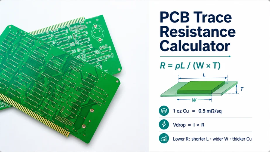
Figure 1. PCB trace resistance affects voltage drop, heat...
PCB Trace Current Capacity: Width, Copper Weight, and IPC-2221
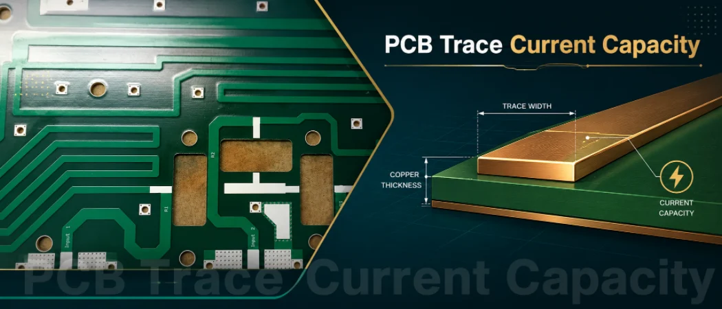
Figure 1. PCB trace current capacity depends on copper...
EAGLE PCB Software: Is It Free, EAGLE vs KiCad, and How to Export Gerber Files
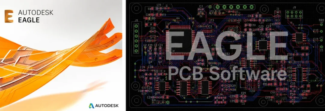
Figure 1. EAGLE PCB software projects should be exported...
Microcontroller Board Soldering and Programming: QFN Pads, SWD, and FTDI Drivers
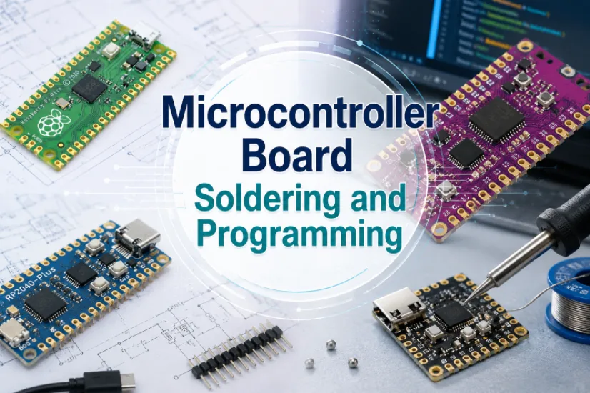
Figure 1. Microcontroller board soldering and programming...
How to get a quote for PCBs
Let‘s run DFM/DFA analysis for you and get back to you with a report. You can upload your files securely through our website. We require the following information in order to give you a quote:
-
- Gerber, ODB++, or .pcb, spec.
- BOM list if you require assembly
- Quantity
- Turn time
In addition to PCB manufacturing, we offer a comprehensive range of electronic services, including PCB design, PCBA, and turnkey solutions. Whether you need help with prototyping, design verification, component sourcing, or mass production, we provide end-to-end support to ensure your project’s success.
For PCBA services, please provide your BOM (Bill of Materials) and any specific assembly instructions. We also offer DFM/DFA analysis to optimize your designs for manufacturability and assembly, ensuring a smooth production process.