
Differences Between HDI PCB and Standard PCB

What Is the Difference Between an HDI PCB and a Standard PCB?
High Density Interconnect (HDI) PCB and standard PCB represent two distinct approaches to printed circuit board design and manufacturing. An HDI PCB utilizes advanced interconnection technologies with higher wiring density, while a standard PCB follows conventional multilayer construction methods. The fundamental difference lies in routing density, via technology, and manufacturing precision.
HDI boards achieve miniaturization through microvias and fine-line traces, whereas standard PCBs rely on through-hole vias and wider trace spacing. The choice between HDI PCB and conventional boards directly impacts product size, signal performance, and manufacturing cost. Modern electronics increasingly demand compact form factors with enhanced functionality, making HDI technology essential for applications where space constraints and electrical performance are critical.
What Are the Basic Structures of HDI PCB and Standard PCB?
Layer Architecture and Via Technology
HDI PCBs typically employ thinner dielectric layers ranging from 50 to 75 microns, compared to standard PCBs that use 100 to 200 micron dielectrics. This structural difference enables HDI boards to incorporate blind vias, buried vias, and stacked microvias with diameters as small as 0.1mm. Standard PCBs predominantly utilize mechanical through-hole vias ranging from 0.2mm to 0.4mm that penetrate the entire board thickness.
The layer count in HDI designs often reaches 8 to 20 layers within compact dimensions, while maintaining circuit density that would require significantly more layers in standard PCB construction. Copper thickness in HDI boards ranges from 0.5oz to 1oz, whereas standard boards commonly use 1oz to 2oz copper to ensure adequate current carrying capacity.
Trace Width and Spacing Specifications
HDI PCB designs achieve trace widths and spacing down to 50 microns or finer, enabling high component pin density and complex routing in constrained areas. Standard PCB manufacturing typically maintains minimum trace widths of 100 to 150 microns with corresponding spacing.
This difference in line geometry directly translates to board size reduction, with HDI technology enabling 40 to 60 percent smaller footprints for equivalent circuit complexity. The compact routing capability of HDI PCB makes it particularly suitable for fine-pitch BGA packages and advanced component technologies that demand precise interconnection geometry.
| Parameter | HDI PCB | Standard PCB |
|---|---|---|
| Via Type | Microvia, Blind, Buried | Through-hole |
| Minimum Via Size | 0.1-0.15mm | 0.2-0.4mm |
| Trace Width/Space | 50-75μm | 100-150μm |
| Dielectric Thickness | 50-75μm | 100-200μm |
| Typical Layer Count | 8-20+ | 4-12 |
How Do HDI PCB and Standard PCB Manufacturing Processes Differ?
Advanced Fabrication Techniques for HDI PCB
HDI PCB manufacturing employs Modified Semi-Additive Process (mSAP) technology, which builds copper traces through electroplating rather than etching away bulk copper. This method enables finer line resolution and improved dimensional accuracy. Laser drilling systems create microvias with precise diameter control and minimal heat-affected zones.
Sequential lamination represents a key distinction in HDI PCB production, where core and buildup layers are pressed in multiple stages rather than a single operation. This approach allows for complex via structures including stacked and staggered microvias that interconnect different layer pairs without penetrating the entire board thickness.
Conventional Manufacturing for Standard PCB
Standard PCB production relies on the Subtractive Process, where manufacturers etch unwanted copper from laminated sheets. Mechanical drilling creates all via holes in a single operation before plating, followed by a single lamination cycle for multilayer boards.
This conventional approach requires less sophisticated equipment and allows for faster throughput with established quality control procedures. The simpler process flow contributes to lower manufacturing costs and shorter lead times for standard PCB production.
Quality Control and Manufacturing Precision
The manufacturing tolerance requirements for HDI PCB are substantially tighter than standard boards. Registration accuracy between layers must maintain tolerances within 50 microns, compared to 100-150 microns for conventional multilayer PCBs.
Each sequential lamination cycle in HDI production introduces additional process variables that require rigorous inspection protocols, including automated optical inspection (AOI) and X-ray examination of buried interconnections. These heightened precision demands necessitate climate-controlled manufacturing environments and specialized equipment, though modern facilities have refined HDI processes to achieve consistent yields.

HDI PCBs
What Are the Key Performance Differences Between HDI PCB and Standard PCB?
Signal Integrity and Electrical Performance
HDI PCB architecture provides superior signal integrity through shortened interconnection paths and reduced via stubs. The smaller via structures minimize parasitic inductance and capacitance, making HDI technology ideal for high-frequency applications operating above 1 GHz.
Impedance control is more precise in HDI designs due to tighter manufacturing tolerances and thinner dielectric materials that reduce signal propagation delays. Standard PCBs with through-hole vias create longer signal paths and introduce greater parasitic effects that can compromise performance in high-speed digital circuits.
The larger via barrels in standard PCB construction act as transmission line discontinuities, causing signal reflections and crosstalk in sensitive applications. However, for circuits operating below 500 MHz, standard PCB construction provides adequate electrical performance without the complexity of HDI routing.
Thermal Management and Mechanical Reliability
HDI structures present thermal management challenges due to thinner copper layers and compact component placement. Thermal vias and heat-spreading layers require careful design integration to prevent hotspot formation.
The microvia interconnections, while electrically superior, exhibit different mechanical stress characteristics under thermal cycling compared to robust through-hole vias in standard PCBs. Standard PCB construction offers proven long-term reliability in harsh environmental conditions, with through-hole plating that withstands repeated thermal expansion cycles.
The thicker copper layers and conventional via structures in standard PCB designs provide better mechanical anchoring for heavy components and improved resistance to vibration and shock loading. Each technology presents distinct advantages depending on the specific operating environment and reliability requirements.
| Performance Aspect | HDI PCB | Standard PCB |
|---|---|---|
| Signal Integrity | Excellent for high-speed | Adequate for moderate speeds |
| Parasitic Effects | Minimized | Higher inductance/capacitance |
| Thermal Management | Requires careful design | Conventional solutions effective |
| Mechanical Durability | Good with proper design | Excellent baseline reliability |
Which Applications Typically Use HDI PCB and Standard PCB?
HDI PCB Application Domains
HDI PCB technology dominates applications where miniaturization combines with high-performance requirements:
- Consumer Electronics – Smartphones and tablets integrate complex functionality within ultra-thin profiles, enabling multiple cameras, processors, and wireless modules in compact assemblies.
- Medical Devices – Wearable biosensors and implantable electronics leverage HDI design to create monitoring circuits in form factors suitable for continuous patient use.
- Aerospace Systems – Radar modules, avionics, and communication equipment employ HDI PCBs where weight reduction and signal performance are paramount.
- Automotive ADAS – Advanced driver assistance systems use HDI technology for sensor fusion processors and camera modules requiring high-speed data processing.
- RF Applications – High-frequency communication systems benefit from the reduced parasitic effects and precise impedance control that HDI structures provide.
Standard PCB Market Segments
Standard PCB construction remains the preferred choice for applications where cost efficiency and proven reliability outweigh extreme miniaturization:
- Industrial Control – PLCs, motor drives, and automation systems utilize conventional multilayer boards for robust performance at competitive pricing.
- Power Electronics – Supply modules and converters benefit from the thicker copper and mechanical stability of standard PCB designs.
- Automotive Body Electronics – Lighting controls, HVAC systems, and infotainment platforms specify standard PCBs for established reliability and manufacturing availability.
- Consumer Appliances – Home electronics, LED drivers, and control interfaces continue to use conventional boards for optimal value.
- General Electronics – Products with relaxed size constraints and moderate signal speeds achieve cost-effective solutions through standard PCB implementation.
Despite the growing adoption of HDI technology, standard PCBs continue to dominate large-volume markets where durability, ease of manufacturing, and cost control remain primary design drivers. Their proven processes and stable supply chain make them an enduring foundation for countless electronic systems across industrial and consumer sectors.

China HDI PCB Manufacturing Services
Why Does HDI PCB Cost More Than a Standard PCB?
HDI PCBs are generally more expensive due to their complex manufacturing processes. Multiple lamination cycles, precise laser drilling, and the mSAP process increase production time and material consumption. Fine-line etching and thin dielectric handling require specialized tooling and slower processing speeds.
Initial yields may be lower than standard PCB manufacturing because of these complexities, though experienced manufacturers can achieve comparable results. Despite higher upfront costs, design strategies—such as applying HDI buildup only in high-density areas—can optimize the balance between performance and cost, and the price gap continues to narrow as HDI production matures.
How to Choose Between an HDI PCB and a Standard PCB?
Design Requirements Assessment
Engineers should evaluate component density, particularly the pin pitch of BGA and CSP packages that may mandate microvia access. Signal integrity requirements drive the decision when designs incorporate high-speed serial interfaces, RF circuits, or precision analog pathways where parasitic effects impact performance.
Product dimensional constraints often determine technology selection, as HDI PCB enables functionality that would be impossible within standard board thickness and area limitations. Budget considerations must account for both manufacturing costs and potential board size reduction that lowers assembly expenses and material consumption.
A design requiring 12 layers with standard PCB technology might achieve equivalent functionality in 8 HDI layers, potentially offsetting the higher per-layer cost through reduced layer count and smaller form factor.
Decision Framework
The selection logic follows this practical approach:
- Choose HDI PCB when – Designs demand high input/output density, operate at signal frequencies above 1 GHz, require miniaturization beyond standard capabilities, or incorporate fine-pitch BGA packages below 0.5mm pitch.
- Choose Standard PCB when – Projects prioritize cost efficiency, have adequate board space, operate at moderate signal speeds below 500 MHz, and use conventional component packages.
- Hybrid Approach – Consider combining HDI buildup layers in critical high-density areas with standard construction elsewhere to balance performance and cost.
Design for Manufacturing Collaboration
Successful HDI PCB implementation requires early engagement with manufacturing partners to establish feasible design rules and stackup configurations. Design for Manufacturing (DFM) analysis identifies potential yield issues before production commitment, optimizing via structures, aspect ratios, and layer transitions for reliable fabrication.
Manufacturers provide design guidelines specific to their process capabilities, ensuring that finished board specifications align with equipment limitations and quality control procedures. This pragmatic collaboration balances technical requirements against economic constraints while maintaining manufacturing feasibility.
Partner With Highleap Electronics for HDI PCB Manufacturing
Highleap Electronics delivers advanced HDI PCB manufacturing capabilities backed by comprehensive quality certifications including ISO9001, IATF16949, and ISO13485. Key capabilities include:
-
Precision Laser Drilling – Achieve microvias and fine-line geometries down to 50 microns with controlled impedance tolerances.
-
mSAP Processing Lines – Support high-density buildup layers with consistent quality and reproducibility.
-
Turnkey PCB & SMT Integration – Combine fabrication and assembly for streamlined supply chains and faster time-to-market.
-
Design-for-Manufacturing Support – Optimize stackup configurations, via structures, and routing strategies to balance performance and manufacturability.
-
High First-Pass Yield – Minimize revision cycles and ensure successful HDI production from prototype to volume manufacturing.
-
Engineering Collaboration – Work with clients to tailor designs for compact, high-performance electronic products.
This structured approach demonstrates Highleap Electronics’ ability to support projects requiring advanced HDI technology while maintaining proven reliability. Contact us to discuss your PCB project now!

Recommended Posts
10 Layer PCB Impedance Control and TDR Verification
Figure 1. 10 layer PCB impedance control coupon and TDR...
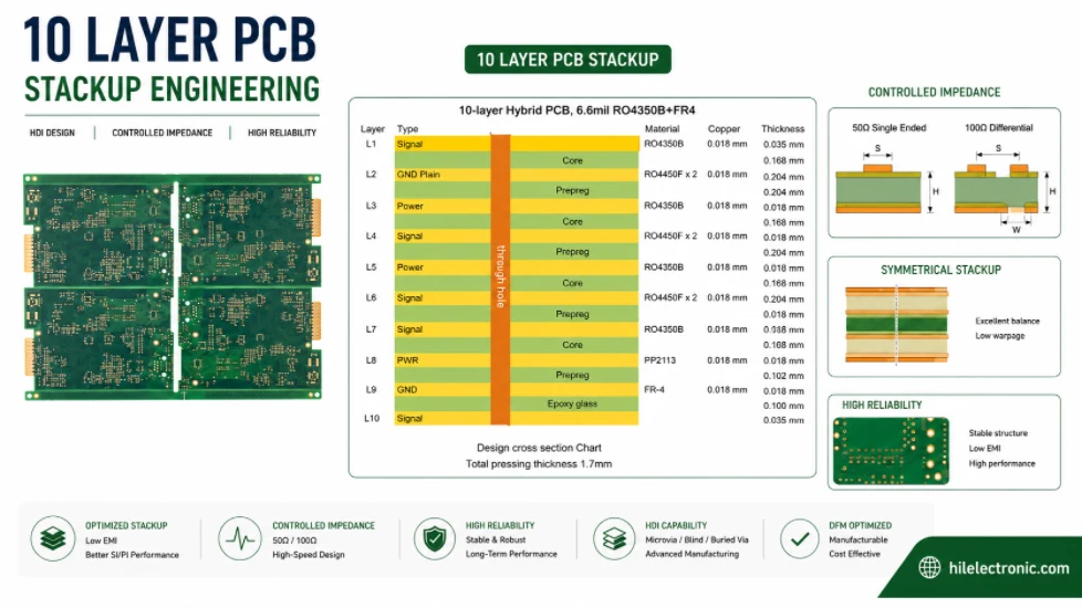
10 Layer PCB Stackup Design for Impedance and Planes
Figure 1. 10 layer PCB stackup for impedance and plane...
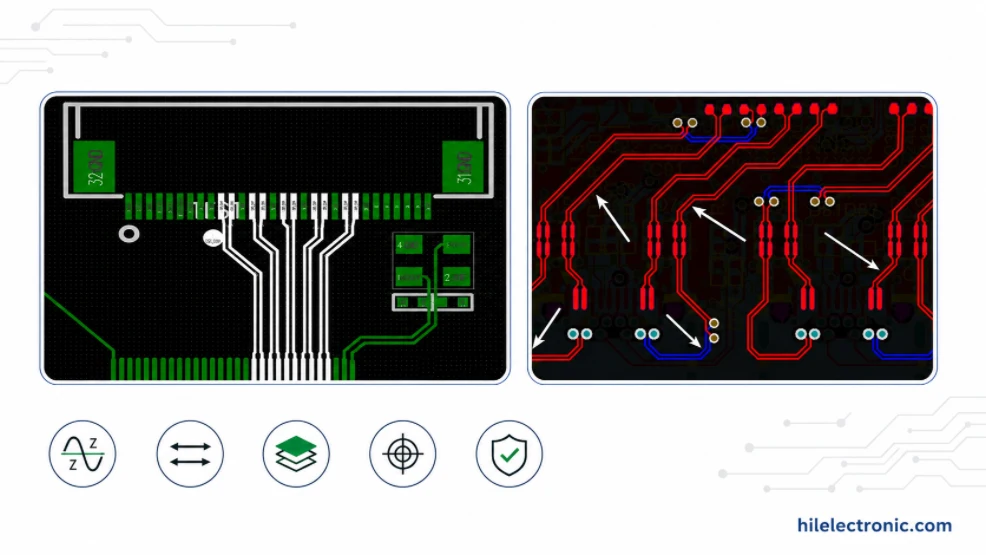
10 Layer PCB Routing Rules for DDR5, PCIe and Crosstalk
Figure 1. 10 layer PCB routing rules for DDR5 PCIe and...
10 Layer PCB Manufacturer for Rigid, Flex and Rigid-Flex
Figure 1. 10 layer PCB manufacturer production capability....
How to get a quote for PCBs
Let‘s run DFM/DFA analysis for you and get back to you with a report. You can upload your files securely through our website. We require the following information in order to give you a quote:
-
- Gerber, ODB++, or .pcb, spec.
- BOM list if you require assembly
- Quantity
- Turn time
In addition to PCB manufacturing, we offer a comprehensive range of electronic services, including PCB design, PCBA, and turnkey solutions. Whether you need help with prototyping, design verification, component sourcing, or mass production, we provide end-to-end support to ensure your project’s success.
For PCBA services, please provide your BOM (Bill of Materials) and any specific assembly instructions. We also offer DFM/DFA analysis to optimize your designs for manufacturability and assembly, ensuring a smooth production process.