
Optimizing Etching and Lamination in Heavy Copper PCB Fabrication

Introduction: Why Etching and Lamination Matter in Heavy Copper PCB Fabrication
Heavy copper PCB fabrication refers to printed circuit boards with copper weights ranging from 3oz to 10oz or higher, significantly exceeding the standard 1-2oz copper thickness found in conventional boards. These boards serve critical applications in power electronics, automotive systems, and industrial equipment where high current carrying capacity and thermal management are essential.
The increased copper thickness introduces substantial manufacturing complexities in heavy copper PCB fabrication. Thicker copper layers amplify etching challenges, with lateral undercut becoming progressively severe as copper weight increases. During lamination, the pronounced surface topology created by thick copper traces disrupts resin flow uniformity, creating opportunities for delamination and void formation. This article examines targeted process optimizations that directly address these challenges and enhance board reliability.
Etching Challenges in Heavy Copper PCB Fabrication
Physical Characteristics of Heavy Copper Etching
Heavy copper etching presents distinct physical challenges rooted in the increased material volume requiring removal. Lateral undercut intensifies proportionally with copper thickness because etchant must penetrate deeper into the material while maintaining vertical attack. This extended exposure time allows horizontal etching to proceed unchecked, compromising trace geometry and dimensional accuracy in heavy copper PCB fabrication.
Line Width Control Issues
Inadequate pattern compensation leads to systematic trace width deviations. Over-etching narrows conductors beyond acceptable tolerances, while under-etching leaves residual copper that can cause shorts. The thick copper mass absorbs etchant unevenly, with areas receiving less spray pressure or lower temperature experiencing slower material removal rates.
Etching Rate Variability Factors
Etchant performance across heavy copper surfaces varies based on copper thickness distribution, fluid dynamics at the board surface, and temperature gradients within the etching chamber. Flow velocity differences between board edges and centers contribute to non-uniform undercut control, requiring careful process parameter management.

Etching
Process Control Techniques for Heavy Copper PCB Etching
Differential and Pulse Etching Methods
Differential etching applies varied etchant concentrations or temperatures to compensate for copper thickness differences across the panel. Pulse etching introduces controlled intervals in the etching cycle, allowing fresh etchant to reach all surfaces uniformly while limiting lateral attack. These techniques maintain vertical etch profiles, reducing undercut severity by 30-40% compared to continuous etching.
Pattern Compensation Strategies
CAM-level pattern compensation adjusts trace widths in the photomask to account for predictable undercut during heavy copper PCB fabrication. Compensation values typically range from 0.1mm to 0.3mm per side, depending on copper weight and etchant system. Software algorithms calculate optimal adjustments based on copper thickness, target line width, and historical etching data.
Spray System Optimization
Nozzle angle adjustment between 15-30 degrees from vertical optimizes etchant impact on thick copper surfaces. Flow rates require calibration to balance material removal speed against undercut control, with higher copper weights demanding reduced velocities. Temperature control systems maintain etchant between 45-50°C with ±2°C stability, ensuring consistent etching rates.
Chemical System Selection
Cupric chloride systems offer superior undercut control for heavy copper PCB fabrication due to their vertical etching characteristics. Alkaline ammonia systems provide faster etch rates but generate more lateral attack. Real-time monitoring of copper ion concentration and specific gravity enables closed-loop process control that maintains optimal etching conditions.
Lamination Techniques for Heavy Copper PCB Fabrication
Core Challenges in Heavy Copper Lamination
The surface topology created by thick copper traces creates barriers to uniform resin flow during lamination. Copper thickness differentials across the panel generate internal stresses that manifest as warpage after cooling. Thermal expansion coefficient mismatches between thick copper layers and epoxy resin systems increase susceptibility to delamination and void formation.
Prepreg Selection and Resin Flow Control
Heavy copper PCB fabrication requires prepreg systems with enhanced flow characteristics to fill the valleys created by thick traces. High-resin-content prepregs with 55-65% resin by weight ensure adequate material availability, while low CTE resin formulations minimize thermal expansion differences. The resin gel time must extend sufficiently to allow complete flow before cure initiation.
Multi-Stage Press Cycles
Staged temperature ramps prevent premature resin gelation while ensuring thorough flow:
- Initial heating to 100-120°C at 2-3°C/minute activates resin flow without triggering cure
- Pressure application follows a graduated profile from 150-200 PSI to 300-350 PSI for consolidation
- Vacuum holds of 5-15 minutes at intermediate temperatures evacuate trapped gases before final cure
- Final cure occurs at 170-180°C to complete resin cross-linking
Registration Control Methods
Layer-to-layer registration in heavy copper PCB fabrication requires pin lamination systems with precise tooling hole alignment. Thermal expansion during press cycles causes greater dimensional movement in thick copper panels, necessitating compensation in tooling hole positioning. Pin diameter tolerances of ±0.025mm and hole position accuracy within ±0.05mm maintain via alignment.

Sequential Lamination
Advanced Lamination Approaches for Heavy Copper PCB Fabrication
Sequential Lamination Process
Sequential lamination builds heavy copper multilayer boards through multiple discrete press cycles, reducing cumulative thermal stress. Inner layer pairs undergo individual lamination before integration into the complete stackup. This approach isolates thick copper layers, allowing optimized press parameters for each sublayer assembly.
Hybrid Copper Thickness Design
Strategic placement of varying copper weights within the stackup balances current carrying requirements against lamination challenges. Power layers utilize heavy copper where needed, while signal layers employ standard weights to reduce topology extremes. This hybrid approach maintains electrical performance while improving resin flow uniformity.
Vacuum-Assisted Lamination
Vacuum lamination systems evacuate air from the stackup before and during pressing, eliminating void precursors. Sustained vacuum of 25-28 inches Hg during the flow stage ensures resin fills all gaps around thick copper features. This technique proves particularly effective for heavy copper PCB fabrication with copper weights exceeding 6oz.
Thermal Press Simulation
Finite element modeling predicts resin flow paths and identifies potential void locations before production. Simulation software accounts for copper thickness distribution, prepreg flow properties, and press cycle parameters to forecast panel behavior. Virtual testing of alternative stackup configurations reduces trial-and-error optimization.
Common Defects and Troubleshooting in Heavy Copper PCB Fabrication
Etching-Related Defects
Excessive lateral undercut creates tapered trace profiles where base widths fall below specification while top widths remain acceptable. Incomplete etching leaves copper residue between traces, particularly in recessed areas with limited etchant access. Etch rate variations across the panel produce trace width inconsistencies that compromise impedance control.
These issues require targeted corrections:
- Etchant system rebalancing to restore optimal copper concentration and pH levels
- Spray bar repositioning to improve flow uniformity across the panel surface
- Pattern compensation adjustments to counteract systematic dimensional shifts
Lamination Defects
Delamination between copper and resin typically results from insufficient surface preparation or inadequate resin flow around thick features. Resin-starved areas appear as white spots on cross-sections, indicating prepreg with insufficient resin content. Panel warpage exceeding 0.75% reflects unbalanced copper distribution or excessive press temperatures.
Corrective Strategies
Stackup design modifications that balance copper weights between top and bottom layers reduce warpage tendencies in heavy copper PCB fabrication. Press pad materials with matched thermal expansion properties support panels during cooling, minimizing stress-induced deformation. Extended vacuum hold times combined with slower heating rates allow thorough degassing before resin gelation.
Conclusion: Process Integration for Reliable Heavy Copper PCB Fabrication
Success in heavy copper PCB fabrication depends on integrated optimization of etching and lamination processes rather than isolated parameter adjustments. The evolution from conventional spray etching toward precision chemical control, combined with advanced multi-stage lamination techniques, has enabled reliable production of boards with copper weights previously considered impractical for volume manufacturing.
Highleap Electronics delivers comprehensive heavy copper PCB fabrication capabilities:
- Copper weight range from 3oz to 20oz with controlled undercut profiles below 15%
- Advanced CAM compensation and pulse etching for dimensional accuracy within ±0.05mm
- Multi-stage vacuum lamination systems ensuring void-free construction
- Sequential and hybrid lamination approaches for complex multilayer stackups
- Full process simulation and optimization for application-specific requirements
Our engineering team provides dedicated support for power conversion, automotive, and industrial control applications. Contact Highleap Electronics to discuss your heavy copper requirements and receive application-specific process recommendations backed by proven manufacturing expertise.

Recommended Posts
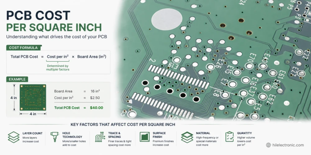
PCB Cost Per Square Inch: What Drives PCB Price and How to Reduce It
Figure 1. PCB cost per square inch image for PCB...
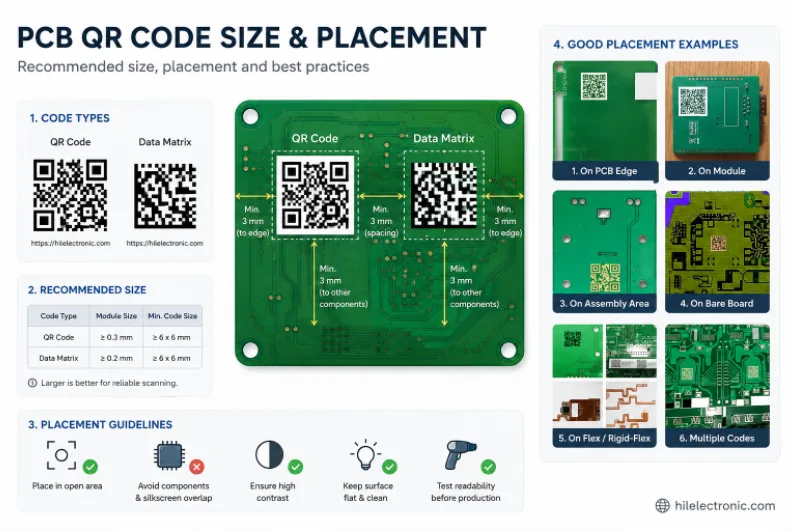
PCB QR Code Size and Placement: Design Rules for Reliable Scanning
Figure 1. PCB QR code size and placement image for PCB...
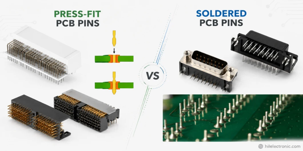
Press-Fit vs Soldered PCB Pins: Header, Connector, and Through-Hole Choices
Figure 1. press-fit vs soldered PCB pins image for PCB...
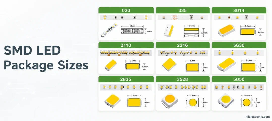
SMD LED Package Sizes: 2835 vs 5050 vs 3528 and PCB Selection
Figure 1. SMD LED package sizes image for PCB...
How to get a quote for PCBs
Let‘s run DFM/DFA analysis for you and get back to you with a report. You can upload your files securely through our website. We require the following information in order to give you a quote:
-
- Gerber, ODB++, or .pcb, spec.
- BOM list if you require assembly
- Quantity
- Turn time
In addition to PCB manufacturing, we offer a comprehensive range of electronic services, including PCB design, PCBA, and turnkey solutions. Whether you need help with prototyping, design verification, component sourcing, or mass production, we provide end-to-end support to ensure your project’s success.
For PCBA services, please provide your BOM (Bill of Materials) and any specific assembly instructions. We also offer DFM/DFA analysis to optimize your designs for manufacturability and assembly, ensuring a smooth production process.