
SMT Stencil: A Complete Guide to Types, Parameters, and Selection

1. Introduction — Define SMT Stencil and Its Role
What Is an SMT Stencil?
An SMT stencil is a thin metal template used in surface mount technology to deposit solder paste onto PCB pads with precision. Typically made from stainless steel, the stencil contains laser-cut apertures that correspond to the pad layout of a circuit board. During the printing process, solder paste is applied across the stencil surface and forced through these openings onto the board below.
Why SMT Stencils Matter in PCB Assembly
The SMT stencil serves a critical function in the solder paste printing stage, which directly influences final solder joint quality. Properly designed stencils ensure consistent paste volume across all pads, reducing common defects such as bridging, insufficient solder, and tombstoning. For high-volume production and fine-pitch component assembly, stencil accuracy becomes essential for achieving reliable, repeatable results.
2. SMT Stencil Types — Classification and Applications
Framed SMT Stencil
A framed SMT stencil is mounted within a rigid aluminum frame under controlled tension. This configuration provides superior stability and precise alignment during automated printing, making it the preferred choice for high-volume production lines. The frame maintains consistent tension across the stencil surface, ensuring uniform paste deposition. However, framed stencils require more storage space and involve higher initial costs.
Frameless SMT Stencil
Frameless SMT stencils offer a cost-effective alternative for prototype development and low-volume production. Without a permanent frame, these stencils are lighter, easier to store, and can be quickly adapted to different PCB designs. They work with universal tensioning systems or manual printing setups. Frameless options are particularly suitable for electronics manufacturers handling diverse, small-batch orders.
Step Stencil
A step stencil features multiple thickness levels on a single template, created through selective etching or electroforming. This design accommodates PCBs with mixed component requirements—delivering more paste for large connectors while reducing volume for fine-pitch ICs on the same board. Step stencils are essential for complex assemblies where uniform thickness cannot satisfy all pad geometries.

Framed SMT Stencils
3. Key SMT Stencil Parameters — Technical Fundamentals
How Stencil Thickness Affects Paste Volume
Stencil thickness directly determines the volume of solder paste deposited on each pad. Thicker stencils transfer more paste, suitable for larger components requiring robust solder joints. Common thickness options range from 0.1mm to 0.2mm, with 0.12mm being standard for most mixed-technology boards. Fine-pitch components (0.4mm pitch or below) typically require thinner stencils to prevent bridging.
Choosing the Right Thickness
Selecting appropriate stencil thickness requires balancing the smallest and largest components on your PCB. When pad size variations are significant, a step stencil or local thickness reduction may be necessary. The goal is achieving optimal paste release for all apertures while maintaining sufficient volume for reliable solder joints after reflow.
Common SMT Stencil Materials
Stainless steel remains the dominant material for SMT stencils due to its durability, corrosion resistance, and compatibility with laser cutting. Most production stencils use 300-series stainless steel, which provides excellent wear characteristics over thousands of print cycles. The smooth surface finish promotes clean paste release and easy cleaning between print runs.
Material Comparison: Steel, Nickel, and Polymer
Electroformed nickel stencils offer superior aperture wall smoothness and are preferred for ultra-fine-pitch applications where paste release is critical. Polymer stencils provide a low-cost option for prototyping or short runs but lack the durability for extended production. Material selection involves trade-offs between precision requirements, production volume, and budget constraints.
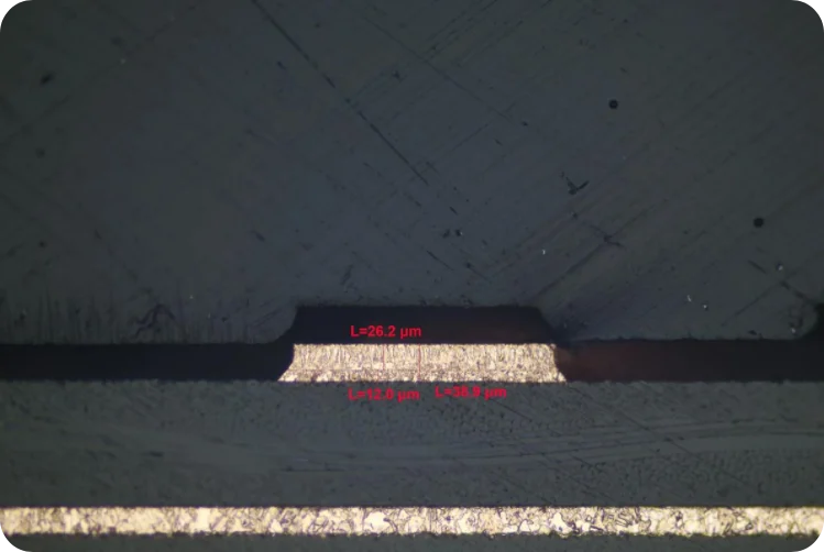
Aperture Size Design
Aperture dimensions must align precisely with PCB pad geometry to ensure proper paste coverage. Oversized apertures cause excess paste and potential bridging; undersized openings result in insufficient solder and weak joints. Standard practice involves reducing aperture size slightly (typically 10-20%) relative to pad dimensions to account for paste spread during squeegee travel.
Area Ratio and Aspect Ratio Considerations
Industry guidelines recommend maintaining an area ratio (aperture area divided by wall area) above 0.66 for reliable paste release. The aspect ratio (aperture width divided by stencil thickness) should exceed 1.5. These metrics, referenced in IPC-7525, help engineers predict whether paste will transfer cleanly from stencil to pad during the printing process.

Step Stencils
4. How SMT Stencil Selection Impacts PCB Assembly Quality
Impact on Solder Joint Quality
Correct SMT stencil selection directly reduces solder defects by ensuring appropriate paste volumes across all pad sizes. Consistent deposition minimizes bridging between adjacent pins and prevents cold or insufficient solder joints. For production environments, proper stencil design translates to higher first-pass yields and reduced rework costs.
Stencil Selection for High-Precision Assembly
High-density boards with fine-pitch components demand careful stencil specification. Factors including aperture geometry, wall smoothness, and thickness uniformity become increasingly critical as component spacing decreases. Matching stencil parameters to design complexity ensures paste release consistency and supports the repeatability required for volume manufacturing.

Frameless SMT Stencil
5. Common Pitfalls and Practical Considerations
Typical Mistakes in SMT Stencil Usage
Common errors include misalignment between stencil apertures and PCB pads, incorrect thickness selection for component mix, and inadequate cleaning schedules. Using damaged or worn stencils leads to inconsistent paste deposits. Failing to verify gerber data against actual pad dimensions before stencil fabrication causes systematic printing defects.
Practical Recommendations for Reliable Printing
Establish regular stencil cleaning intervals based on paste type and print frequency. Maintain proper squeegee pressure and speed settings for consistent results. Verify stencil tension before production runs, particularly for framed configurations. Review paste layer data during design output to catch aperture sizing issues before manufacturing begins.
6. Summary
The SMT stencil is a fundamental component in surface mount assembly, directly influencing solder paste deposition accuracy and final joint quality. Understanding the distinctions between framed, frameless, and step stencil configurations enables appropriate selection for specific production requirements. Key parameters—thickness, material, and aperture design—must be optimized according to PCB complexity and component specifications.
Proper stencil selection reduces defects, improves yield consistency, and supports efficient high-volume manufacturing. By avoiding common pitfalls and following established design guidelines, manufacturers can maximize the performance of their solder paste printing process and achieve reliable assembly results.

Recommended Posts
Prepreg Material for Multilayer PCB Manufacturing
On this page Understanding Core and Prepreg Materials...
Low Loss PCB Fabrication for High-Speed Digital and RF Applications
On this page What Is Low Loss PCB Fabrication When Do You...

PCB Laminate Lead Time and Production Scheduling
On this page Why Laminate Lead Times Vary Standard vs...
Low Dk Low Df PCB Material for High Speed Signals
Figure 1. Low loss PCB material selection for high speed...
How to get a quote for PCBs
Let‘s run DFM/DFA analysis for you and get back to you with a report. You can upload your files securely through our website. We require the following information in order to give you a quote:
-
- Gerber, ODB++, or .pcb, spec.
- BOM list if you require assembly
- Quantity
- Turn time
In addition to PCB manufacturing, we offer a comprehensive range of electronic services, including PCB design, PCBA, and turnkey solutions. Whether you need help with prototyping, design verification, component sourcing, or mass production, we provide end-to-end support to ensure your project’s success.
For PCBA services, please provide your BOM (Bill of Materials) and any specific assembly instructions. We also offer DFM/DFA analysis to optimize your designs for manufacturability and assembly, ensuring a smooth production process.