
Exploring the Significance of PCB Stencils

In the world of printed circuit board assembly (PCBA), precision is paramount. As the demand for smaller, more complex electronic devices grows, so does the need for accurate and efficient assembly processes. PCB stencils are one of the key tools that make this possible. These stencils play an essential role in applying solder paste precisely where it’s needed, ensuring the reliable performance of the finished product. In this article, we’ll delve into the significance of PCB stencils, explore their role in surface mount technology (SMT), and provide best practices for optimizing your PCBA projects.
What is a PCB Stencil?
A PCB stencil, also known as a solder paste stencil, is a critical tool used in the PCB assembly process. Its primary function is to ensure the precise and uniform application of solder paste onto the PCB before surface-mount devices (SMD components) are placed. Here’s a step-by-step look at how PCB stencils work:
- Alignment: The PCB stencil is carefully aligned on the PCB, with its openings (apertures) perfectly matching the solder pads on the PCB. Proper alignment is crucial for ensuring that the solder paste is deposited accurately.
- Solder Paste Application: A specialized solder paste, which is a mixture of solder alloy and flux, is applied to the stencil’s surface. This paste is what will eventually form the electrical connections between components and the PCB.
- Pressure Application: A squeegee or automated stencil printer is used to press the solder paste through the stencil apertures. The pressure ensures that the solder paste is deposited onto the PCB pads in precise amounts.
- Precise Deposition: The solder paste is deposited onto the PCB in a controlled manner, following the pattern defined by the stencil’s openings. This precise deposition is essential for creating reliable solder joints once the components are placed and reflowed.
PCB stencils are typically made from thin sheets of stainless steel or nickel, chosen for their durability and precision. The apertures in the stencil are meticulously crafted to match the exact locations of the solder pads and component footprints on the PCB. Regular cleaning and maintenance of the stencil are necessary to ensure its longevity and the quality of the solder paste application. Overall, PCB stencils are indispensable for achieving high-quality, consistent results in PCB assembly.
Why Solder Paste Stencils Are Essential in Electronics Manufacturing
Solder paste stencils are not just tools—they are critical components in the electronics manufacturing process. The use of these stencils is driven by the need for precision, consistency, and efficiency in the production of electronic devices. Here are several reasons why solder paste stencils are indispensable:
-
Ensuring High-Quality Standards: The electronics industry is known for its stringent quality requirements. Solder paste stencils help manufacturers achieve these high standards by ensuring the consistent and precise deposition of solder paste. This reduces the risk of soldering defects such as bridges or voids, leading to more reliable electronic assemblies.
-
Consistency in Solder Paste Application: One of the biggest challenges in PCB assembly is maintaining consistency across multiple boards. Solder paste stencils ensure that the right amount of paste is applied to each solder pad, resulting in uniform solder joints across the entire PCB. This consistency is crucial for the reliability and performance of the final product.
-
Supporting Fast Turnaround Times: In today’s fast-paced electronics market, manufacturers often face tight deadlines. Solder paste stencils, especially when used in automated SMT assembly lines, enable rapid and efficient PCB assembly. This speed is vital for meeting market demands and delivering products on time.
-
Enabling Large-Scale Production: As electronics manufacturing scales up, the ability to produce large volumes of PCBs quickly and efficiently becomes more important. Solder paste stencils facilitate this by supporting high-volume production runs without sacrificing quality or precision.
-
Reducing Material Waste and Costs: Solder paste is a valuable material, and using stencils helps minimize waste by ensuring that only the necessary amount of paste is applied. This not only reduces material costs but also minimizes the need for post-process cleanup.
-
Process Optimization and Control: In any manufacturing environment, process control is key to maintaining quality and efficiency. Solder paste stencils contribute to this by providing a controlled, repeatable method for applying solder paste, making it easier to identify and correct issues in the assembly process.

Key Features of High-Quality PCB Stencils
To maximize the effectiveness of your PCB stencils, it’s important to focus on the key elements that determine their performance. Here’s a closer look at the features that make for a high-quality PCB stencil:
-
Frame: The frame of a stencil provides the necessary support and stability during the solder paste printing process. Frames are typically made from durable materials like aluminum or stainless steel, which maintain their shape and integrity throughout multiple uses. A well-constructed frame ensures consistent pressure application and alignment, both of which are critical for accurate paste deposition.
-
Apertures: Apertures are the openings in the stencil through which the solder paste is applied to the PCB. The size, shape, and placement of these apertures are precisely matched to the solder pads on the PCB. Proper aperture design is crucial for ensuring the correct amount of solder paste is deposited, which is essential for forming reliable solder joints.
-
Tensioning Mechanism: Some stencil frames incorporate tensioning mechanisms, such as tensioning bars or screws, to maintain the stencil’s flatness and tension. This feature is vital for achieving uniform solder paste deposition across the entire PCB, which directly impacts the quality and reliability of the solder joints.
-
Foil: The stencil’s foil, usually made of stainless steel or nickel, is selected for its durability, precision, and resistance to wear. The thickness of the foil is chosen based on the size of the components and the volume of solder paste required. Thinner foils are often used for finer pitch components, where precise paste application is critical.
The PCB Stencil Manufacturing Process
The manufacturing process for PCB stencils is a meticulously executed sequence of steps that directly impacts the quality and performance of the final product. Each stage of the process is critical in ensuring that the stencil meets the exacting standards required for PCB assembly. Here’s an overview of the stencil manufacturing process:
- Design Preparation: The first step in stencil manufacturing is the design preparation phase. During this stage, the stencil design is created based on the PCB layout. The design must precisely define the aperture sizes and shapes to ensure accurate solder paste deposition. Factors such as component size, solder paste volume requirements, and assembly specifications are considered during the design process.
- Material Selection: After the design is finalized, the next step is selecting the material for the stencil. The choice of material significantly affects the stencil’s durability and performance. Common materials include stainless steel, known for its strength and corrosion resistance, and nickel, valued for its mechanical properties and longevity.
- Fabrication: The stencil is then fabricated using one of two common methods: laser cutting or chemical etching. Laser cutting is highly precise, using a focused laser beam to create clean, smooth apertures. Chemical etching involves using a chemical process to remove material and create the desired apertures, offering excellent accuracy for complex designs.
- Cleaning and Inspection: Once fabricated, the stencil undergoes rigorous cleaning to remove any residues or contaminants. This step is crucial for ensuring optimal solder paste release during the printing process. The stencil is also inspected to verify its quality, with any imperfections addressed before it is used in PCB assembly.
- Framing or Mounting: Stencils are typically thin sheets and may require additional support for stability and precise alignment during use. Frames made of materials like aluminum or stainless steel are used to provide this support and help align the stencil accurately with the PCB pads.
- Stencil Printing: The final step is using the stencil in the PCB assembly process. Solder paste is applied to the stencil, and a squeegee or stencil printer is used to spread the paste evenly across the apertures. The paste is then deposited onto the PCB pads, setting the stage for component placement.
- Maintenance: To ensure consistent performance, regular maintenance of the stencil is necessary. This includes routine cleaning to remove any solder paste residues and periodic inspection to check for wear or damage. Proper maintenance extends the stencil’s lifespan and ensures the quality of the solder paste application remains high.
How CAM Engineers Create the Necessary Files for PCB Stencils
CAM engineers are responsible for generating the necessary files for PCB stencils based on the provided Gerber files from the customer. If the customer has included the stencil layer in the Gerber files, the CAM engineer will use these files directly, ensuring that they carefully compare and verify the details. Any discrepancies or issues found during the comparison process will be confirmed with the customer for clarification. This step is crucial to ensure the stencil file is accurate and matches the customer’s design specifications.
In cases where the customer has not provided a stencil layer, the CAM engineer will create the stencil file based on the company’s standards and specifications. If the order involves panelized boards (multi-board panel delivery), the engineer will convert the stencil files into the company’s panel format. In addition, the engineer will add necessary features such as fiducial marks and alignment holes on the panel. Special attention must be given to the alignment holes to ensure they follow the foolproof design (poka-yoke) principles to prevent assembly errors, ensuring the stencils are aligned correctly during production.
How to Choose the Right PCB Stencil for Your Production Needs
Selecting the right PCB stencil is crucial for optimizing the PCB assembly process. The requirements for different production environments, component sizes, and solder paste types can significantly influence the choice of stencil. Several factors should be taken into account when choosing a stencil that best suits your specific needs.
1. Component Type and Size
The type and size of components being used are central to stencil selection. For high-density components, such as fine-pitch devices, precise stencil apertures are necessary to ensure the accurate application of solder paste. In contrast, larger components may require wider apertures to accommodate larger amounts of solder paste. The precision of the stencil’s apertures plays a crucial role in the reliability of the final solder joints.
2. Production Volume
The scale of your production is another important factor. For small-batch production, the need for frequent stencil replacements may be lower, and cost considerations often drive stencil selection. However, in large-scale production environments, durability becomes a priority. Stencils used in high-volume production need to withstand more frequent use and maintain their integrity over extended periods, ensuring consistent solder paste deposition.
3. Solder Paste Type
Different solder pastes, such as lead-free or leaded solder paste, vary in consistency and particle size. These variations require different stencil designs to ensure that solder paste is applied evenly and accurately. For instance, thicker pastes may require slightly larger apertures to accommodate the material flow, while finer pastes demand more precision in stencil aperture size and placement.
4. Pad Design and Layer Count
For multilayer PCBs, solder paste must be applied with precision to ensure proper connection across different layers of the board. This involves careful design to ensure solder paste flows smoothly across all layers without obstructing vias or misaligning the pads. The added complexity of multilayer boards often requires stencils that are designed to accommodate these intricate connections.
5. Budget Considerations
The budget available for stencils can influence the materials and fabrication methods chosen. Higher-quality stencils, such as those made from stainless steel or nickel, offer greater durability and precision but come at a higher cost. For some production environments, finding a balance between cost and quality is essential, especially when considering factors like production volume and frequency of stencil use.
Conclusion
In the fast-paced world of electronics manufacturing, achieving precision and reliability is key. At Highleap Electronic, we understand that high-quality PCB stencils play a crucial role in the success of your PCB assembly process. These stencils ensure the accurate application of solder paste, which is vital for creating reliable and high-performance circuit boards.
By choosing Highleap Electronic for your PCB manufacturing and assembly needs, you’re partnering with a company that prioritizes quality, efficiency, and consistency. Our advanced manufacturing techniques, combined with the use of high-precision PCB stencils, ensure that your assemblies meet the rigorous standards required by today’s electronics industry.
Whether you are scaling up production, improving product quality, or optimizing your manufacturing processes, Highleap Electronic is the partner you need to achieve your goals. Our expertise in PCB assembly, coupled with the use of top-quality PCB stencils, will help you stay competitive and deliver exceptional results in a rapidly evolving market.
FAQ
1. What is the role of a PCB stencil in the assembly process?
A PCB stencil plays a critical role in ensuring the precise and uniform application of solder paste on a printed circuit board (PCB). It helps create the electrical connections between components and the PCB by applying solder paste accurately onto the pads before components are placed, ensuring the reliability and functionality of the final product.
2. How does the PCB solder paste stencil market impact electronics manufacturing?
The PCB solder paste stencil market has seen significant growth as the demand for more complex and compact electronic devices rises. These stencils are essential in high-precision applications, allowing manufacturers to meet quality standards and production efficiency. As the market expands, advancements in stencil technology continue to improve the consistency and speed of solder paste application, crucial for large-scale electronics production.
3. What are the best practices for cleaning stencil openings during the assembly process?
Cleaning stencil openings is vital for ensuring consistent solder paste application. Regular cleaning prevents paste buildup, ensuring that each aperture remains clear. It’s recommended to use non-abrasive cleaning materials, such as lint-free wipes and alcohol-based solvents, to gently clean the stencil. Avoid harsh chemicals that could damage the material or affect the stencil’s precision. Cleaning should be done after each use to maintain stencil integrity and performance.
4. How does the quality of a stencil affect PCB assembly?
The quality of a stencil directly impacts the precision and uniformity of solder paste deposition on the PCB. High-quality stencils made from durable materials, such as stainless steel or nickel, ensure that solder paste is accurately applied to the solder pads, reducing defects like bridges or voids. Consistent solder paste application is crucial for reliable connections and optimal performance of the assembled PCB.
5. Why is maintaining stencil apertures important in PCB manufacturing?
Maintaining clean and precise stencil apertures is essential for achieving high-quality PCB assemblies. As the apertures wear over time, they can become clogged with solder paste or suffer from misalignment, leading to inconsistent paste deposition. Regular inspection and cleaning of stencil apertures help ensure that they remain accurate, minimizing the risk of defects and ensuring that the PCB assembly process runs smoothly.
Get a Free PCB & PCBA Quote

Recommended Posts
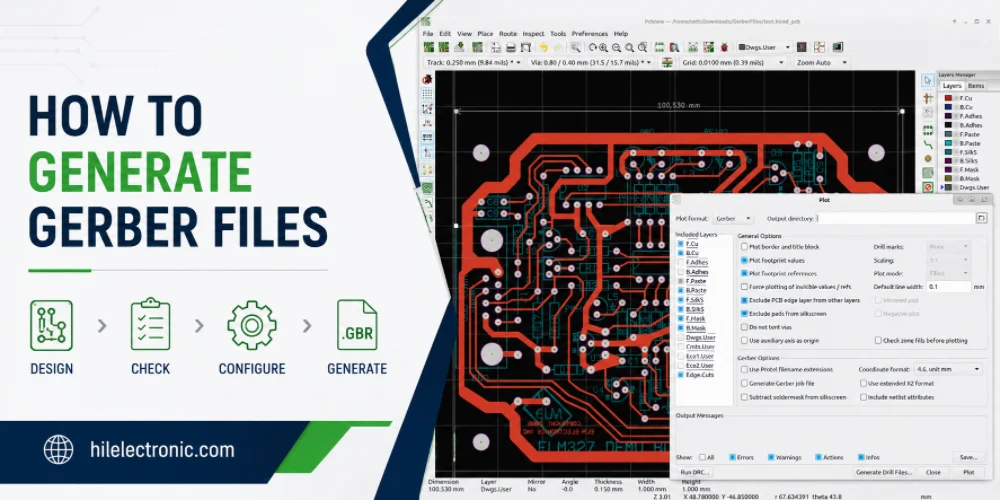
How to Generate Gerber Files for PCB Manufacturing
Figure 1. how to generate Gerber files image for Highleap...
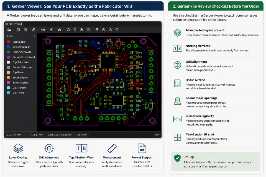
Gerber File Review Checklist: How to Check PCB Files Before You Order
Figure 1. Gerber file review catches missing layers, drill...
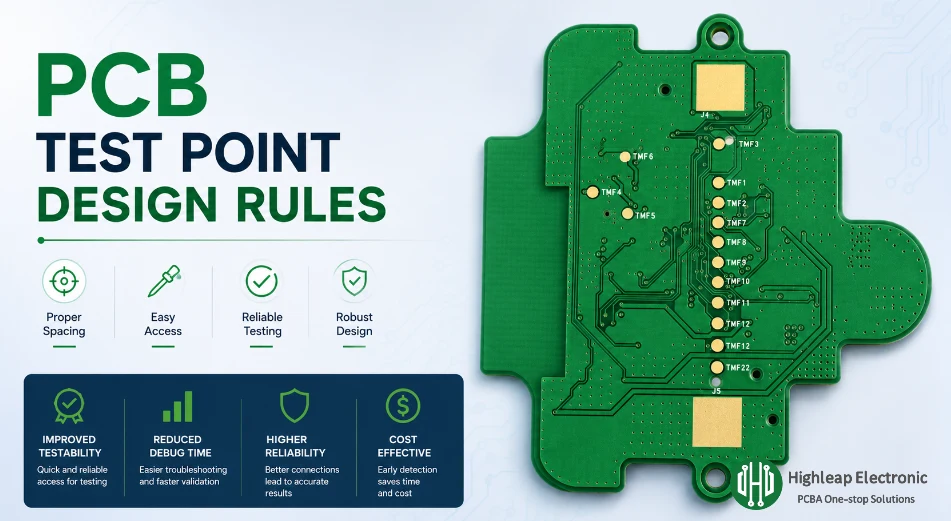
PCB Test Point Design Rules for Debug and ICT
Figure 1. PCB test point design rules help make debugging,...

PCB Jumper Wire: Uses, Types, and Design Tips
Figure 1. PCB jumper wires are useful for prototypes and...
How to get a quote for PCBs
Let us run DFM/DFA analysis for you and get back to you with a report.
You can upload your files securely through our website.
We require the following information in order to give you a quote:
-
- Gerber, ODB++, or .pcb, spec.
- BOM list if you require assembly
- Quantity
- Turn time
In addition to PCB manufacturing, we offer a comprehensive range of electronic services, including PCB design, PCBA (Printed Circuit Board Assembly), and turnkey solutions. Whether you need help with prototyping, design verification, component sourcing, or mass production, we provide end-to-end support to ensure your project’s success. For PCBA services, please provide your BOM (Bill of Materials) and any specific assembly instructions. We also offer DFM/DFA analysis to optimize your designs for manufacturability and assembly, ensuring a smooth production process.