
China PCB Manufacturing Price Per Square Inch Guide

PCB pricing based on square inches provides a useful starting point for cost estimation, but the relationship between board area and price is more complex than simple multiplication. Understanding how manufacturers calculate area-based pricing helps optimize board dimensions and estimate budgets more accurately.
Table of Contents
At Highleap Electronics, we help customers understand how board dimensions affect manufacturing economics. This guide explains the relationship between PCB size and cost, including factors that simple square-inch calculations miss.
1. How PCB Area Pricing Works
PCB manufacturers often express pricing in terms of cost per square inch as a simplified reference. However, this metric represents just one dimension of a complex pricing structure.
1.1 The Basic Calculation
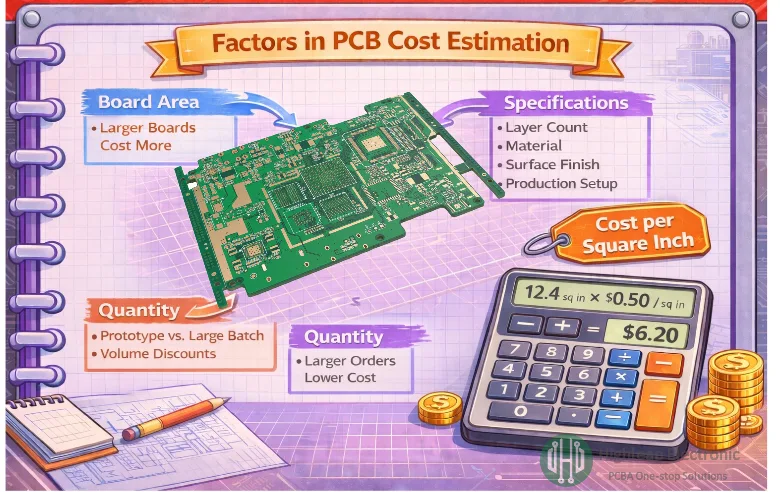
Board area in square inches = Length (in) × Width (in)
For a 100mm × 80mm board:
- Convert to inches: 3.94″ × 3.15″ = 12.4 square inches
- At $0.50 per square inch: 12.4 × $0.50 = $6.20 per board
This baseline calculation assumes standard specifications. Actual pricing adjusts based on layer count, material selection, surface finish, minimum features, and production volume.
1.2 Typical Price Ranges by Specification
For standard 2-layer FR-4 at production volumes, prices typically run $0.03-0.08 per square inch. 4-layer boards range from $0.08-0.15 per square inch. 6-layer boards cost $0.15-0.25 per square inch, and 8+ layer boards run $0.25-0.50+ per square inch.
These ranges assume standard specifications (1oz copper, HASL finish, 6/6 mil features). Premium specifications increase these baselines significantly.
For prototype quantities, multiply production pricing by 3-5× due to setup cost amortization. See our PCB fabrication cost guide for complete cost factor analysis.
1.3 Minimum Order Charges
Most manufacturers have minimum order values regardless of board size. A very small board might have a theoretical square-inch cost of $2, but if minimum order charges are $50, that’s the actual floor price.
Typical minimum charges range from $30-100 for prototypes, $100-300 for small batches, and are negotiable for production volumes.
2. Calculating Your Board’s Square Inch Cost
Understanding how to estimate your specific board’s price-per-area helps with budgeting and design optimization.
2.1 Step-by-Step Calculation
Step 1: Calculate board area
- Rectangular: Length × Width
- Irregular: Use bounding rectangle (smallest rectangle enclosing the shape)
- For mm dimensions: Area (sq in) = Area (sq mm) ÷ 645.16
Step 2: Determine base price tier
- Layer count establishes baseline
- Consult manufacturer or use ranges above
Step 3: Apply specification multipliers
- Non-standard materials: 1.2-5× multiplier
- Heavy copper: 1.1-1.5× multiplier
- Advanced features: 1.2-2× multiplier
- Premium finish: 1.1-1.3× multiplier
Step 4: Adjust for volume
- Prototype (5-10 pcs): 3-5× production price
- Small batch (50-100 pcs): 1.5-2× production price
- Production (1,000+ pcs): baseline price
2.2 Example Calculation
For a 4-layer, 50mm × 50mm board with ENIG finish at 100-piece quantity:
- Area: 1.97″ × 1.97″ = 3.88 square inches
- 4-layer base rate: $0.12/sq in
- ENIG multiplier: 1.25×
- Small batch multiplier: 1.75×
- Price estimate: 3.88 × $0.12 × 1.25 × 1.75 = $1.02 per board
Actual quotes may vary—this provides estimation only.
3. Panel Utilization: The Hidden Factor
The relationship between board size and cost isn’t linear because manufacturers produce boards on standard-size panels. Panel utilization significantly affects actual cost.
3.1 Manufacturing Panel Sizes
Standard manufacturing panels are typically 18″ × 24″ (457mm × 610mm) or 21″ × 24″ (533mm × 610mm). Your board must fit within these dimensions including routing borders (typically 5-10mm per edge), handling rails (10-15mm for automation), and fiducials and tooling holes.
3.2 How Utilization Affects Cost
Consider two boards with identical square inch area but different dimensions:
Board A: 100mm × 100mm (15.5 sq in)
- Panel fit: 4 × 5 = 20 boards per panel
- Utilization: 72%
Board B: 50mm × 200mm (15.5 sq in)
- Panel fit: 2 × 8 = 16 boards per panel
- Utilization: 58%
Same area, but Board A costs ~20% less due to better panel utilization.
3.3 The “Sweet Spot” Dimensions
Certain board dimensions optimize panel utilization. Near-square aspect ratios (length within 1.5× of width) generally utilize better. Dimensions that divide evenly into panel size waste less material. Standard sizes like 100×100mm, 50×100mm, and 100×150mm typically offer good utilization.
4. When Square Inch Pricing Breaks Down
Simple area-based calculations fail to capture several important cost factors.
4.1 Very Small Boards
Boards under 1 square inch don’t follow linear pricing. Handling difficulty increases—small boards are harder to process. Minimum charges dominate as setup costs can’t amortize. Panel border ratios become unfavorable since proportionally more space goes to borders.
A 10mm × 10mm board might cost the same as a 25mm × 25mm board despite being 1/6 the area.
4.2 Very Large Boards
Boards approaching panel size have different economics. Yield risk increases as larger boards have more area for defects. Processing limitations emerge since some equipment has size limits. Panel efficiency drops if board doesn’t divide evenly.
4.3 Irregular Shapes
Non-rectangular boards are priced on bounding rectangle, meaning the smallest rectangle that contains the entire board shape. A circular board with 100mm diameter uses the same panel area as a 100mm × 100mm square, despite having 21% less actual board area.
Complex routing adds cost beyond simple edge routing. Internal cutouts require additional processing.
4.4 Complexity Factors
Features that increase cost independently of area include high layer counts (pricing scales steeper than area), fine features (require more expensive processes regardless of size), controlled impedance (adds processing regardless of board size), and special testing (some tests charge per board, not per area).
5. Optimizing Board Dimensions for Cost
Practical strategies for dimension optimization during design:
5.1 Design Phase Considerations
- Start with panel awareness: Know target panel size before finalizing dimensions
- Consider standard sizes: 50mm, 100mm, 150mm increments often fit panels well
- Allow flexibility: If function allows, design dimensions with 5-10% flexibility
- Minimize waste: A slightly larger board that fits more per panel costs less
5.2 Aspect Ratio Guidelines
- Optimal: 1:1 to 1:1.5 (square to slightly rectangular)
- Acceptable: 1:1.5 to 1:2
- Problematic: Beyond 1:3 (long narrow boards waste panel space)
5.3 Working with Your Manufacturer
Ask your manufacturer about their standard panel sizes, panelization recommendations for your board, price impact of dimension adjustments, and multi-design panel options for prototypes.
Highleap Electronics provides panelization consultation to help optimize dimensions for cost-effective manufacturing.
6. Getting Accurate Pricing Beyond Square Inches
While square inch calculations provide estimates, accurate pricing requires complete specifications.
6.1 Information Needed for Accurate Quotes
- Complete dimensions: Length, width, thickness, tolerances
- Layer stackup: Layer count, copper weights, dielectric requirements
- Materials: Laminate type, Tg requirements, special properties
- Features: Minimum trace/space, smallest drill, via types
- Finish: Surface finish type, thickness requirements
- Quality: IPC class, testing requirements
- Quantity: Order quantity and expected annual volume
- Timing: Required PCB lead time
6.2 Beyond Bare Board Cost
For complete project budgeting, consider:
- Assembly costs: Component placement and soldering (see PCB assembly cost)
- Component costs: Often larger than board and assembly combined
- Testing costs: Based on test coverage requirements
- Logistics: Shipping, handling, import duties if applicable
Our PCBA cost breakdown guide provides comprehensive total project cost analysis.
6.3 Getting Started with Highleap Electronics
For accurate pricing on your specific project:
- Submit Gerber files and specifications through our quote portal
- Receive detailed quote within 24 hours
- Review panelization recommendations
- Discuss optimization opportunities with engineering team
For expedited PCB manufacturing or projects with specific PCB MOQ requirements, our team provides customized solutions.
Contact us today for a detailed quote based on your actual requirements—not just square inch estimates.
Helen supports international engineering teams with end-to-end PCB fabrication and assembly solutions, helping projects move from quick-turn prototypes to stable mass production. Her experience spans high-frequency and RF boards, complex multilayer stackups, rigid-flex, and flex PCB technologies across multiple industries. By translating technical requirements into practical manufacturing plans, she helps customers improve manufacturability, reduce risk, and optimize cost and lead time—while maintaining consistent quality at scale.
at Highleap Electronics

Recommended Posts
10 Layer PCB Routing Rules for DDR5, PCIe and Crosstalk
Figure 1. 10 layer PCB routing rules for DDR5 PCIe and...
10 Layer PCB Manufacturer for Rigid, Flex and Rigid-Flex
Figure 1. 10 layer PCB manufacturer production capability....
10 Layer AI Server PCB Engineering for Accelerator Hardware
Figure 1. 10 layer AI server PCB for accelerator hardware....
10 Layer PCB Cost Drivers for Materials, HDI and Testing
Figure 1. 10 layer PCB cost drivers for materials HDI and...
How to get a quote for PCBs
Let us run DFM/DFA analysis for you and get back to you with a report.
You can upload your files securely through our website.
We require the following information in order to give you a quote:
-
- Gerber, ODB++, or .pcb, spec.
- BOM list if you require assembly
- Quantity
- Turn time
In addition to PCB manufacturing, we offer a comprehensive range of electronic services, including PCB design, PCBA (Printed Circuit Board Assembly), and turnkey solutions. Whether you need help with prototyping, design verification, component sourcing, or mass production, we provide end-to-end support to ensure your project’s success. For PCBA services, please provide your BOM (Bill of Materials) and any specific assembly instructions. We also offer DFM/DFA analysis to optimize your designs for manufacturability and assembly, ensuring a smooth production process.