
Aluminum PCB Cost Reduction: Strategic Approaches to Manufacturing Efficiency

Introduction
Aluminum PCBs have become indispensable in high-power electronics and LED lighting applications due to their superior thermal dissipation capabilities and mechanical stability. These metal core printed circuit boards efficiently transfer heat away from critical components, extending product lifespan and improving reliability. However, rising raw material prices and energy costs have placed increasing pressure on manufacturers and designers to optimize production expenses without compromising performance.
Achieving effective aluminum pcb cost reduction requires a comprehensive understanding of the entire value chain, from initial design decisions through final assembly. This article examines practical strategies that address material selection, manufacturing processes, and supply chain integration to maintain competitive pricing while delivering the thermal management performance that demanding applications require.
Understanding Major Cost Factors in Aluminum PCB Production
The foundation of aluminum pcb cost optimization begins with identifying the primary expense drivers throughout the manufacturing process. Material costs typically represent 40-50% of total production expenses, with aluminum substrate thickness, copper foil weight, and dielectric layer specifications directly impacting unit prices.
Material-Related Cost Drivers
The aluminum base layer, thermally conductive dielectric layer, and copper circuit layer each contribute differently to overall expenses. Standard configurations use 1.0-2.0mm aluminum substrates with 1-3 oz copper weights, while the dielectric layer selection significantly influences both thermal performance and cost. Premium dielectric materials with higher thermal conductivity can increase material costs by 30-100% compared to standard options.
Process Complexity Factors
Single-layer aluminum PCBs offer straightforward manufacturing economics, while special requirements such as contoured routing, precision drilling, or advanced surface finishes like ENIG or immersion silver add incremental processing steps. Copper distribution patterns affect etching time, while dense thermal via arrays increase drilling costs and require careful process control to maintain yield rates.
Production Volume Impact
Larger batch sizes enable better material utilization and reduced setup time per unit, creating economies of scale. Production yields directly multiply costs, as a manufacturing line operating at 95% yield produces five defective units per hundred, while improvement to 98% yield reduces defects to two per hundred. Identifying these mcpcb production cost factors is essential for effective aluminum pcb cost reduction strategies.

Material Optimization Strategies for Aluminum PCB Cost Reduction
Strategic material selection delivers substantial opportunities for aluminum pcb cost optimization without compromising essential thermal characteristics. The relationship between dielectric thermal conductivity and system-level temperature management often allows for more economical material choices than initial specifications suggest.
Dielectric Layer Selection
Standard dielectric materials with 1.0 W/mK thermal conductivity serve moderate power applications effectively at the lowest cost point. Enhanced formulations providing 2.0 W/mK thermal conductivity command a 30-40% premium and become cost-effective when junction temperatures approach critical limits. High-performance options reaching 3.0 W/mK or higher justify their cost only in extreme power density scenarios where thermal resistance directly limits system performance.
Copper Thickness Optimization
Circuit current requirements and thermal spreading needs can often be satisfied with 1 oz copper for low-power applications or 2 oz copper for moderate power levels, representing optimal material optimization in aluminum pcb. Each doubling of copper weight increases material costs by approximately 20% and extends etching time. Designers should calculate actual current density requirements rather than defaulting to heavier copper weights based on assumptions.
Aluminum Base Material Selection
The industry standard 1.6mm thickness serves most applications effectively, balancing thermal performance with mechanical rigidity. Thinner 1.0mm options reduce material costs by 20-25% for designs where external housings provide mechanical support. Thicker 2.0mm substrates benefit applications requiring enhanced flatness but should be specified only when engineering analysis supports the requirement.
Supply Chain Advantages
Consolidating material procurement with qualified suppliers generates cost advantages through volume pricing and reduced inventory carrying costs. Long-term supply agreements provide price stability that enables accurate project costing while ensuring material availability during supply chain disruptions.
Implementing Design for Manufacturability for Aluminum PCB Cost Reduction
Design for manufacturability principles directly influence aluminum pcb manufacturing cost by aligning circuit design with efficient manufacturing processes. Early collaboration between design engineers and manufacturing specialists identifies potential cost drivers before tooling investment occurs, preventing expensive redesign cycles.
Circuit Layout Optimization
Optimizing component placement to minimize board area reduces material consumption proportionally while potentially allowing more circuits per production panel. Standardizing trace widths and spacing according to manufacturer capabilities eliminates premium processing charges associated with fine-line requirements that exceed standard tolerances.
Thermal Via Strategy
Thermal vias improve heat conduction from components to the aluminum base, but excessive via density increases processing time without proportional thermal benefits. Thermal simulation identifies the minimum viable via count that meets temperature specifications, reducing unnecessary drilling operations and supporting pcb design optimization for cost objectives.
Panel Utilization
Designing board dimensions that fit efficiently within standard panel sizes maximizes the number of circuits per panel, distributing setup and processing costs across more units. Even small dimensional adjustments can improve panel utilization from 70% to 85%, directly reducing per-unit costs through better material yield.
Standardization Benefits
Limiting the variety of specifications across product families streamlines manufacturing operations:
- Hole size standardization – Reduces tool changes and setup time between production runs.
- Common board thicknesses – Enables batching similar products for lamination cycles.
- Unified surface finishes – Eliminates process interruptions that reduce throughput efficiency.
- Shared material specifications – Aggregates purchasing volume for better supplier pricing.

Enhancing Manufacturing Process Efficiency for Cost Optimization
Process efficiency improvements deliver measurable aluminum pcb cost optimization through reduced cycle times and enhanced first-pass yields. Modern aluminum PCB manufacturing facilities employ automated equipment for photoresist application, exposure, and development to ensure consistent processing parameters while increasing throughput capacity.
Lamination Process Control
Temperature control during lamination proves critical for preventing delamination and warpage issues that create scrap or require expensive rework. Precision heating profiles ensure complete bonding between the dielectric layer and both aluminum and copper layers. Manufacturers with sophisticated lamination presses and real-time monitoring systems achieve yields exceeding 98% for standard aluminum PCB constructions.
Quality Inspection Integration
Quality inspection systems integrated throughout the manufacturing process catch defects early when correction costs remain minimal. Automated optical inspection identifies copper pattern defects immediately after etching, while electrical testing verifies circuit continuity and isolation before assembly. These quality gates prevent defective boards from advancing through subsequent processing steps where value addition would be wasted.
Continuous Improvement Impact
Leading aluminum PCB manufacturers implement statistical process control programs that systematically identify and eliminate sources of variation. Regular analysis of defect patterns reveals opportunities for equipment calibration, process parameter refinement, or handling procedure improvements. These incremental enhancements compound over time to create sustainable cost advantages that support long-term aluminum pcb cost reduction goals.
Supply Chain Integration for Aluminum PCB Cost Control
Integrated supply chain approaches enable significant cost reduction through improved coordination and reduced transaction costs. Manufacturers offering comprehensive services from bare board fabrication through component assembly eliminate multiple handoffs that introduce delays, potential quality issues, and additional overhead expenses.
Strategic Supplier Partnerships
Long-term partnerships with material suppliers provide advance notice of price changes and opportunities for collaborative cost reduction initiatives. Supplier integration and cost control practices establish stable pricing frameworks that protect against raw material volatility. Manufacturers with established supply networks can often absorb minor material cost fluctuations without immediately passing increases to customers.
Domestic vs Offshore Considerations
While offshore manufacturing may offer lower labor costs, total landed costs include shipping, customs duties, inventory carrying costs, and longer lead times. For many aluminum PCB applications, domestic or regional manufacturing provides better total cost of ownership when factoring in reduced inventory requirements and faster response to engineering changes.
Volume Aggregation Benefits
Consolidated purchasing across multiple product lines creates volume leverage that individual projects cannot achieve independently:
- Material cost advantages – Aggregate demand for aluminum substrates and dielectric materials secures preferential pricing.
- Inventory efficiency – Shared material specifications reduce safety stock requirements across product families.
- Supplier relationship depth – Higher total volumes strengthen negotiating position for quality and delivery terms.
Engineering Collaboration Value
Experienced manufacturing partners contribute expertise that identifies cost reduction opportunities invisible to design teams working in isolation. Design review services catch potential manufacturing challenges before prototyping, while material selection guidance ensures specifications align with actual performance requirements rather than overspecified margins.
Conclusion
Aluminum pcb cost reduction emerges from systematic attention to design decisions, material selection, manufacturing efficiency, and supply chain optimization rather than any single intervention. The most significant opportunities arise from material optimization matched to actual thermal requirements, design for manufacturability principles that align circuit layouts with efficient processing, and manufacturing partnerships that deliver both technical expertise and economies of scale.
Highleap Electronics Capabilities
As an experienced PCB manufacturer and assembly provider, Highleap Electronics delivers comprehensive aluminum pcb cost optimization through integrated capabilities:
- Material expertise – Technical guidance on dielectric selection and copper thickness optimization based on thermal simulation and application requirements.
- DFM collaboration – Early design review services that identify cost reduction opportunities before prototyping investment.
- Process efficiency – Automated manufacturing equipment and rigorous quality control systems achieving yields exceeding 98%.
- Supply chain integration – Consolidated services from bare board fabrication through component sourcing and assembly, reducing coordination overhead and total project costs.
- Volume advantages – Established supplier relationships and aggregated purchasing power that translate into competitive pricing for customers.
Partner with Highleap Electronics
By partnering with Highleap Electronics, you gain access to manufacturing expertise and process control necessary to deliver cost-effective aluminum PCB solutions without compromising the thermal management performance your applications demand. Contact our engineering team today to discuss how our integrated approach can optimize both performance and cost for your next aluminum PCB project.

Recommended Posts

NP-175F PCB Laminate for High-Reliability Multilayer Boards
NP-175F PCB laminate is a Nan Ya high-Tg, filled...

High CTI FR-4 PCB Manufacturing for Insulation-Critical Boards
High CTI FR-4 is used when a PCB design needs stronger...
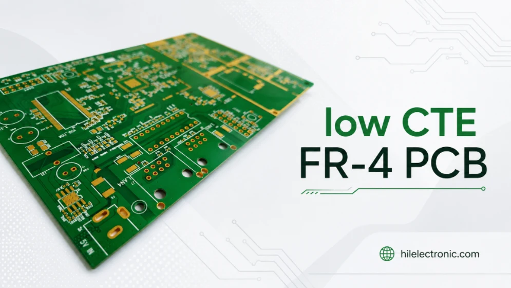
Low CTE FR-4 PCB Manufacturing for Through-Hole Reliability
Low CTE FR-4 PCB manufacturing is used when a circuit...
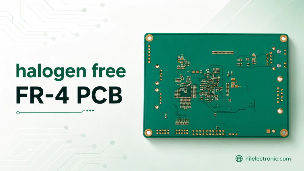
Halogen Free FR-4 PCB Manufacturing for Controlled Material Builds
Halogen free FR-4 PCB manufacturing is used when a product...
How to get a quote for PCBs
Let‘s run DFM/DFA analysis for you and get back to you with a report. You can upload your files securely through our website. We require the following information in order to give you a quote:
-
- Gerber, ODB++, or .pcb, spec.
- BOM list if you require assembly
- Quantity
- Turn time
In addition to PCB manufacturing, we offer a comprehensive range of electronic services, including PCB design, PCBA, and turnkey solutions. Whether you need help with prototyping, design verification, component sourcing, or mass production, we provide end-to-end support to ensure your project’s success.
For PCBA services, please provide your BOM (Bill of Materials) and any specific assembly instructions. We also offer DFM/DFA analysis to optimize your designs for manufacturability and assembly, ensuring a smooth production process.