
Aluminum PCB Defects: Common Issues and Prevention Strategies

Understanding Aluminum PCB Defects in High-Power Applications
Aluminum PCBs have become essential in high-power electronic devices, LED lighting systems, and power modules where efficient heat dissipation is critical. However, aluminum pcb defects can significantly compromise reliability and performance in these thermal management applications. The unique construction of metal core PCBs introduces specific failure modes that differ from traditional FR-4 boards, making defect prevention crucial for manufacturers and design engineers working with automotive, industrial, and consumer electronics.
Critical Aluminum PCB Defects: Delamination Issues
Causes of Delamination in Aluminum PCB
Delamination represents one of the most severe aluminum pcb defects, occurring when copper foil separates from the dielectric layer or when the dielectric detaches from the aluminum base. This failure stems from excessive thermal stress during soldering, inadequate adhesion between laminated layers, or prolonged thermal cycling exposure. Visible copper trace lifting, circuit opens, and compromised electrical isolation indicate delamination problems.
Preventing Delamination Defects
Prevention requires strict control of reflow soldering temperature profiles, ensuring peak temperatures remain within material specifications. Key prevention strategies include:
- Temperature control – Maintain reflow profiles below dielectric glass transition temperature to prevent stress-induced separation.
- Material selection – Use high-quality lamination materials with appropriate thermal ratings for your application environment.
- Press optimization – Control lamination pressure, temperature, and dwell time to ensure complete bonding between layers.
Aluminum PCB Defects: Solder Joint Problems
Common Solder Joint Issues in MCPCB
Solder joint integrity poses unique challenges in metal core PCB assemblies due to aluminum’s high thermal conductivity. Common solder joint issues in mcpcb include cold solder joints, bridging between adjacent pads, and insufficient wetting caused by rapid heat dissipation. These defects result from improper reflow curves that fail to account for the aluminum base’s thermal mass, pad surface oxidation, or incompatible solder alloy selection.
Solutions for Solder Joint Defects
Implementing precise thermal profiling with extended soak zones compensates for the substrate’s heat-sinking effect. Surface finishes such as ENIG or immersion silver provide superior solderability compared to HASL, while lead-free solder paste formulated for thermal management applications ensures consistent joint formation across the assembly.
Warping and Bending: Structural Aluminum PCB Defects
Understanding Warping in Aluminum PCB
Board warpage constitutes a significant PCB quality issue affecting assembly yield and long-term reliability. Warping in aluminum pcb occurs due to unbalanced thermal expansion between copper, dielectric, and aluminum layers, or asymmetric copper distribution across the board surface. Uneven heating during reflow exacerbates these stresses, resulting in bow or twist that complicates component placement and may cause solder joint cracking over time.
Preventing Warpage Defects
Design and manufacturing strategies minimize warpage potential:
- Symmetrical design – Balance copper patterns and weight distribution across both board surfaces.
- Thickness control – Select appropriate aluminum base thickness (1.5mm to 3.0mm) based on board size and thermal requirements.
- Uniform heating – Implement controlled reflow profiles with even heat distribution and proper board support during thermal operations.

PCB Warpage
Thermal Stress and Overheating Aluminum PCB Defects
Thermal Stress PCB Problems in High-Power Applications
Excessive thermal stress represents a persistent challenge where component power density concentrates heat in localized areas. Thermal stress pcb problems manifest as accelerated dielectric aging, thermal fatigue of solder joints, and eventual delamination under repeated cycling. Insufficient heat spreading or inadequate aluminum thickness fails to manage thermal loads effectively in demanding applications.
Thermal Management Solutions
Prevention begins at the design phase with thermal simulation to identify hot spots and optimize component placement. Increasing aluminum substrate thickness enhances heat spreading capability, while incorporating thermal vias in high-power component areas improves vertical heat transfer. Proper thermal interface material selection between the PCB and heatsink ensures efficient system-level heat dissipation.
Surface Treatment and Etching Aluminum PCB Defects
Common Surface and Etching Defects
Surface treatment and circuit etching defects directly impact solderability and electrical performance. Issues include incomplete copper etching leaving residual shorts, over-etching that narrows traces beyond tolerance, and surface oxidation degrading pad solderability. These defects arise from inconsistent etching solution concentration, inadequate process control, or excessive time between fabrication and assembly.
Quality Control for Surface Defects
Automated optical inspection systems catch etching irregularities early in production. Controlled impedance etching processes with real-time monitoring maintain dimensional accuracy, while protective surface finishes applied immediately after etching prevent oxidation. Storage in low-humidity environments with moisture barrier packaging preserves surface quality until assembly operations.
Preventing Aluminum PCB Defects: Integrated Quality Strategies
Material and Process Controls
Effective defect prevention integrates material selection with process engineering throughout manufacturing. High-grade aluminum substrates with certified dielectric systems provide the foundation for reliable boards. Critical controls include:
- Lamination parameters – Maintain press temperature, pressure, and timing within validated windows for consistent bonding.
- Reflow validation – Verify temperature profiles using actual board thermal measurements, not oven settings alone.
- Cleanliness protocols – Ensure contamination-free processing to prevent adhesion and solderability failures.
Advanced Inspection Methods
Automated optical inspection identifies surface anomalies and dimensional variations, while X-ray inspection reveals internal delamination and voiding in thermal vias. Flying probe testing verifies electrical continuity without fixture requirements, particularly valuable for prototype and low-volume production runs.
Design for Manufacturing
Design for manufacturability principles applied during layout prevent many aluminum pcb defects before production begins. Adequate spacing between high-current traces prevents thermal crosstalk, while proper pad sizing accommodates the aluminum substrate’s thermal characteristics. Controlled copper balancing across panel layouts minimizes warpage potential from the design stage.
Highleap Electronics: Manufacturing Excellence in Aluminum PCBs
Specialized expertise in metal core PCB fabrication proves essential for consistently preventing aluminum PCB defects. Highleap Electronics combines precision lamination equipment, validated thermal management processes, and comprehensive quality verification to deliver reliable aluminum PCBs for demanding applications. Our engineering team collaborates with customers during design review to identify potential manufacturability issues early in the development cycle.
Years of experience in high-power LED drivers, automotive power modules, and industrial control systems inform our process optimization approaches. We maintain strict controls across lamination, imaging, etching, and surface finishing operations with real-time monitoring and statistical validation.
Conclusion: Proactive Aluminum PCB Defect Prevention
Understanding and preventing aluminum pcb defects requires comprehensive knowledge of materials, processes, and application requirements. The defects discussed including delamination, solder joint issues, warping, thermal stress problems, and surface defects each demand specific prevention strategies throughout design and manufacturing. Proactive defect prevention through proper material selection, validated processes, and thorough inspection delivers far greater value than reactive troubleshooting and rework.
Ready to eliminate aluminum PCB defects in your next project? Highleap Electronics offers customized metal core PCB solutions with comprehensive engineering support. Contact our technical team to discuss your thermal management requirements and discover how our proven manufacturing processes deliver defect-free aluminum PCBs for demanding applications.

Recommended Posts

NP-175F PCB Laminate for High-Reliability Multilayer Boards
NP-175F PCB laminate is a Nan Ya high-Tg, filled...

High CTI FR-4 PCB Manufacturing for Insulation-Critical Boards
High CTI FR-4 is used when a PCB design needs stronger...
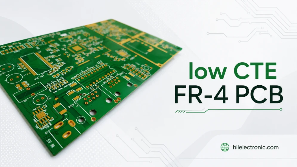
Low CTE FR-4 PCB Manufacturing for Through-Hole Reliability
Low CTE FR-4 PCB manufacturing is used when a circuit...
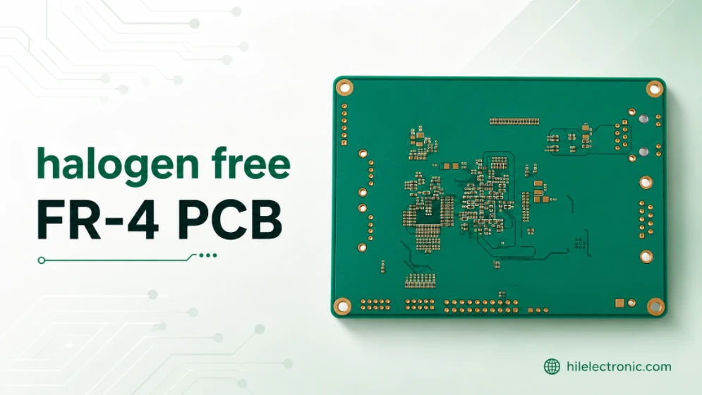
Halogen Free FR-4 PCB Manufacturing for Controlled Material Builds
Halogen free FR-4 PCB manufacturing is used when a product...
How to get a quote for PCBs
Let‘s run DFM/DFA analysis for you and get back to you with a report. You can upload your files securely through our website. We require the following information in order to give you a quote:
-
- Gerber, ODB++, or .pcb, spec.
- BOM list if you require assembly
- Quantity
- Turn time
In addition to PCB manufacturing, we offer a comprehensive range of electronic services, including PCB design, PCBA, and turnkey solutions. Whether you need help with prototyping, design verification, component sourcing, or mass production, we provide end-to-end support to ensure your project’s success.
For PCBA services, please provide your BOM (Bill of Materials) and any specific assembly instructions. We also offer DFM/DFA analysis to optimize your designs for manufacturability and assembly, ensuring a smooth production process.