
Circuit Board Thickness: A Comprehensive Guide

Understanding Circuit Board Thickness in Manufacturing
In the field of electronics manufacturing, the thickness of circuit boards is a critical specification that influences both performance and cost. While there is no universally recognized standard for circuit board thickness, certain dimensions have become widely accepted within the industry. These preferred thicknesses facilitate smoother design processes, optimize manufacturing efficiency, and help control costs. Variations in circuit board thickness are common, and designers often select custom thicknesses based on specific project requirements. This guide will clarify what constitutes “standard” circuit board thickness and provide insights on how to determine the most suitable thickness for your project.
Defining Standard Circuit Board Thickness
The industry often recognizes 0.062 inches (1/16 inch) as the standard circuit board thickness, typically with a tolerance of 10%. This thickness emerged from historical manufacturing practices involving Bakelite sheets. While 0.062 inches is the most commonly used thickness, other dimensions such as 0.031 inches and 0.093 inches are also prevalent, particularly for multilayered or more robust boards. Although circuit boards can come in a range of thicknesses, these measurements are generally accepted as standard.
Factors Influencing Circuit Board Thickness
Determining the appropriate circuit board thickness involves assessing various design and manufacturing factors, which can be categorized as follows:
Design Factors
-
- Size, Weight, and Flexibility
Thinner boards are lighter and more flexible but may sacrifice structural integrity. Conversely, thicker boards provide enhanced durability but add weight and occupy more space, which can be disadvantageous in compact applications. The intended use of the board significantly influences these considerations. - Copper Thickness
The thickness of the copper layer impacts overall board thickness and is determined by the current load requirements. Standard copper thickness typically ranges from 1.4 to 2.8 mils (1 to 2 oz), but it can be adjusted based on specific design needs. - Board Materials
The choice of materials used for the substrate and laminate directly affects the thickness of the circuit board. Common materials include epoxy resin, glass weave, and thermoset resin, each influencing the board’s thermal, mechanical, and electrical properties. - Number of Layers
The complexity of the circuit board, represented by the number of layers, affects thickness. While designs with 2 to 6 layers can often meet standard thicknesses, boards requiring 8 or more layers generally necessitate increased thickness. - Signal Types
Different signal types carried by the circuit board can dictate material requirements and subsequently influence thickness. High-power signals require thicker copper and wider traces, leading to a thicker board, while high-density boards often utilize thinner materials. - Types of Vias
The density and type of vias (e.g., through vias, micro vias) also affect the required thickness. Micro vias can be effectively used in thinner boards due to their smaller size. - Operating Environment
The operational conditions, including exposure to temperature and humidity, impact conductivity and resistance. Thicker boards may be preferred in harsher environments for enhanced durability, while thinner boards are more suitable for applications requiring flexibility.
- Size, Weight, and Flexibility
Manufacturing Factors
In addition to design considerations, manufacturing capabilities play a vital role in determining circuit board thickness:
-
- Drill Hole Equipment
The precision of drill holes is limited by board thickness and the capabilities of the manufacturing equipment. Understanding the aspect ratio (the ratio of hole depth to diameter) is essential in assessing achievable specifications. - Copper Processing
The processes used to create copper traces—such as etching and plating—are influenced by the thickness of the internal copper layer, which can affect manufacturability and costs. - Layer Count
Increasing the number of layers complicates manufacturing and often necessitates thicker boards. Specialty manufacturers may offer solutions for thinner layers, but this capability varies and may incur higher costs. - Depanelization Method
The method for separating PCBs from manufacturing panels can depend on thickness. Thicker boards might require careful scoring, while thinner boards may be routed for easier separation.
- Drill Hole Equipment
For related manufacturing decisions, Highleap also documents LED aluminum PCB production and Rogers PCB manufacturing, which can help prevent unclear notes in the quote package.
Key Considerations for Choosing Circuit Board Thickness
When determining the optimal circuit board thickness for your project, several critical factors must be taken into account to ensure the final product meets both performance and manufacturing requirements:
1. Manufacturer Capabilities
Understanding the capabilities of your manufacturer is essential. Each manufacturer has unique equipment, processes, and expertise that may influence the feasibility of achieving your desired thickness. Early and clear communication with the manufacturer helps to establish whether they can meet your specifications, including tolerances and dimensional requirements.
2. Turnaround Time
The complexity of custom thicknesses can significantly impact manufacturing timelines. Adjusting equipment settings and processes for unique specifications may introduce delays. It is important to discuss the expected turnaround time early in the design phase to manage project schedules effectively. Understanding the lead times associated with both standard and custom thicknesses will help in planning product launches and ensuring timely delivery.
3. Cost Implications
The financial aspects of circuit board thickness should not be overlooked. Custom thicknesses typically involve higher production costs due to specialized materials and manufacturing processes. A thorough cost-benefit analysis is advisable, comparing the advantages of custom solutions against the potential savings of standard thickness options. Evaluating the total cost of ownership—including manufacturing, materials, and long-term performance—can provide valuable insights for your decision-making process.
By carefully considering these factors, you can make informed decisions regarding circuit board thickness that align with your project goals and manufacturing capabilities. For tailored advice and support, consulting with experienced PCB manufacturers can further enhance your design and production processes.

PCBA one-stop turnkey service
Conclusion
Choosing the right circuit board thickness is a multifaceted decision influenced by various design and manufacturing considerations. While standard thicknesses can simplify the manufacturing process and reduce costs, there are numerous scenarios where custom thicknesses are essential for achieving optimal performance in specialized applications.
Custom PCB thickness allows for tailored solutions that can enhance the functionality and reliability of your product. Engaging with an experienced PCB supplier can provide valuable insights and support, ensuring that your unique specifications are met efficiently. With the right partner, you can leverage the benefits of both standard and custom options to optimize your project’s success.
Get a Free PCB & PCBA Quote

Recommended Posts
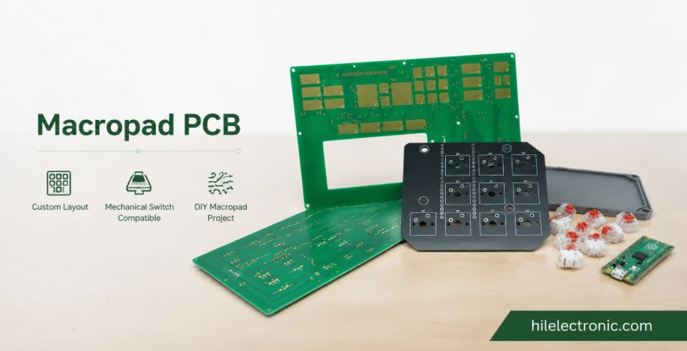
Macropad PCB Manufacturing & Custom PCBA
Table of contentsMacropad PCB Buying Guide and Quick...
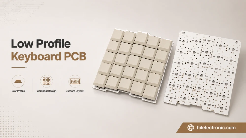
Low-Profile Keyboard PCB Manufacturing & Assembly
Table of contentsLow Profile and Choc Keyboard PCBA...

Keyboard PCBA Testing & Firmware Programming
Table of contentsKeyboard PCB Functional Testing Scope and...

Hall Effect Keyboard PCB Manufacturing & PCBA
Table of contentsHall Effect Keyboard PCB Buying...
How to get a quote for PCBs
Let us run DFM/DFA analysis for you and get back to you with a report.
You can upload your files securely through our website.
We require the following information in order to give you a quote:
-
- Gerber, ODB++, or .pcb, spec.
- BOM list if you require assembly
- Quantity
- Turn time
In addition to PCB manufacturing, we offer a comprehensive range of electronic services, including PCB design, PCBA (Printed Circuit Board Assembly), and turnkey solutions. Whether you need help with prototyping, design verification, component sourcing, or mass production, we provide end-to-end support to ensure your project’s success. For PCBA services, please provide your BOM (Bill of Materials) and any specific assembly instructions. We also offer DFM/DFA analysis to optimize your designs for manufacturability and assembly, ensuring a smooth production process.