
Excellent Quality Camera PCB Manufacturing in China

In today’s rapidly evolving technological landscape, the demand for high-quality camera PCBs (Printed Circuit Boards) is at an all-time high. These essential components play a critical role in various applications, especially in indoor and outdoor security systems. This article delves into the intricacies of camera PCB manufacturing, highlighting the advanced processes and technologies that ensure superior performance and reliability.
The Importance of Camera PCBs
Camera PCBs are pivotal components in surveillance systems, providing essential electrical connections for imaging modules, sensors, and other critical elements. A well-designed PCB enhances image quality, minimizes signal loss, and ensures the durability of security systems. As surveillance technology advances, the design and manufacturing of these circuit boards must also evolve to meet higher standards.
Camera PCBs are integral to various applications, including CCTV systems, smart home security devices, industrial monitoring systems, and high-tech military applications. Each of these fields has unique requirements that demand innovative solutions. For instance, military-grade camera PCBs must withstand extreme conditions, including temperature fluctuations, humidity, and shock, while maintaining operational integrity.
Camera PCB Key Manufacturing Process
Design and Prototyping
The journey of a camera PCB begins with meticulous design and prototyping. Engineers utilize advanced Computer-Aided Design (CAD) software to create intricate layouts that optimize space and performance. The design phase involves careful consideration of factors such as signal integrity, power distribution, and thermal management. Rapid prototyping techniques, including 3D printing and CNC machining, allow for quick iterations and testing of designs, ensuring they meet specific requirements before full-scale production.
Material Selection
The choice of materials is critical for the performance of camera PCBs. High-frequency materials, such as FR-4, Rogers, and polyimide, are commonly used to support signal integrity and minimize interference. The substrate must withstand environmental challenges, especially in outdoor applications where moisture, temperature variations, and UV exposure can significantly affect performance. Selecting the right solder mask and surface finish is also essential for enhancing durability and ensuring reliable connections.
Fabrication Techniques
State-of-the-art fabrication techniques are employed to produce camera PCBs. Precision drilling and laser cutting ensure that each PCB is manufactured to exact specifications. Etching techniques remove unwanted copper, creating the necessary circuit pathways while minimizing waste. Multi-layer designs can incorporate complex circuitry that allows for advanced functionalities in compact spaces. Automated processes enhance accuracy and reduce manufacturing time, enabling quicker turnaround for customers while maintaining quality.
Assembly Processes
After fabrication, the assembly of components is crucial. Advanced soldering techniques, including surface mount technology (SMT) and through-hole soldering, ensure secure connections. The assembly process often involves placing numerous small components, which requires precision and efficiency. Automated pick-and-place machines guarantee consistent placement of components, minimizing the risk of human error and increasing production speed. Additionally, the use of reflow soldering ovens ensures that solder is properly melted and cooled, creating strong, reliable joints.
Testing and Quality Assurance
Rigorous testing protocols are essential to ensure the reliability of camera PCBs. This includes electrical testing, where each PCB is checked for shorts, opens, and proper functioning of all components. Thermal cycling tests simulate environmental stress, ensuring that PCBs can withstand extreme temperature variations. Environmental stress tests evaluate the PCB’s performance under conditions such as humidity and UV exposure. Quality assurance measures verify that each PCB meets industry standards, providing peace of mind to manufacturers and end-users alike. Certifications such as ISO 9001 and IPC-A-610 ensure that manufacturing processes are consistently refined and meet stringent quality benchmarks.
Excellent Quality Camera PCB Manufacturing in China
China has emerged as a global leader in the manufacturing of high-quality camera PCBs, driven by a combination of advanced technology, skilled labor, and cost-effective production processes. The country’s robust electronics manufacturing ecosystem facilitates the creation of sophisticated camera PCBs that meet the demanding standards of various industries, including security, automotive, and consumer electronics.
1. Advanced Manufacturing Technologies
Chinese manufacturers leverage cutting-edge technologies, such as automated assembly lines, precision machining, and advanced material science. The implementation of Industry 4.0 practices, including smart factories and real-time data analytics, ensures efficiency and quality control throughout the production process. This technological edge allows for the rapid scaling of production while maintaining stringent quality standards.
2. Comprehensive Supply Chain Integration
China’s well-established supply chain ecosystem plays a pivotal role in camera PCB manufacturing. Local sourcing of materials, components, and machinery reduces lead times and costs, enabling manufacturers to respond swiftly to market demands. The proximity of component suppliers fosters collaboration and innovation, leading to improved design iterations and faster prototyping.
3. Skilled Workforce and Expertise
The success of camera PCB manufacturing in China is underpinned by a highly skilled workforce. Engineers and technicians are trained in the latest PCB design and manufacturing techniques, ensuring that they are well-equipped to tackle complex challenges. Continuous education and training programs help maintain a competitive edge in an ever-evolving industry.
4. Commitment to Quality Assurance
Chinese manufacturers prioritize quality assurance at every stage of production. Stringent testing protocols, including electrical, thermal, and environmental assessments, ensure that each camera PCB meets or exceeds international standards. Certifications such as ISO 9001 and IPC-A-610 demonstrate a commitment to quality and reliability, providing customers with confidence in their products.
5. Customization Capabilities
The ability to provide tailored solutions is a significant advantage for Chinese PCB manufacturers. Whether catering to consumer electronics, industrial applications, or military-grade equipment, manufacturers can customize designs to meet specific client requirements. This flexibility not only enhances customer satisfaction but also fosters long-term partnerships.
6. Competitive Pricing and Global Reach
Competitive pricing without compromising quality makes Chinese manufacturers attractive to global clients. By offering high-quality products at lower costs, Chinese companies can penetrate diverse markets, from North America to Europe and beyond. This global reach is further supported by established logistics and distribution networks, ensuring timely delivery and support.
For businesses seeking reliable, high-quality camera PCBs, China offers a compelling solution that delivers exceptional value and innovative designs. By choosing us, you can enhance the performance and capabilities of your imaging systems, ensuring your products stand out in a competitive market. Partner with us to leverage cutting-edge technology and elevate your security solutions!
If this requirement affects sourcing or production release, compare it with PCB quality assurance process and bare board electrical test before sending the final files for review.

Customization for Diverse Applications
Camera PCBs can be tailored to meet the specific needs of various applications. Whether for high-resolution indoor cameras or robust outdoor surveillance systems, customization options such as size, layer count, and component selection allow manufacturers to provide solutions that cater to diverse requirements.
For instance, high-resolution cameras may require PCBs with multiple layers to accommodate advanced imaging technologies. Compact designs for smart home devices might prioritize minimal size and weight without compromising functionality. Custom PCB designs also allow for the integration of features like motion sensors, night vision capabilities, and wireless connectivity, which are increasingly becoming standard in modern security systems.
The Role of Supporting Algorithms and Circuit Boards in Camera PCB Applications
To fully leverage the capabilities of camera PCBs in high-tech devices, the integration of advanced algorithms and complementary circuit boards is crucial. Modern imaging systems demand not only precision hardware but also sophisticated software solutions to optimize image processing, enhance data analysis, and facilitate real-time decision-making.
Advanced Algorithms for Image Processing
Algorithms play a pivotal role in transforming raw data captured by camera sensors into meaningful insights. Techniques such as machine learning and computer vision are increasingly employed to enhance image clarity, reduce noise, and improve object detection and recognition. For instance, convolutional neural networks (CNNs) are utilized to analyze visual data, allowing for feature extraction and classification with remarkable accuracy. These algorithms must be optimized to run efficiently on the limited processing power available on embedded systems, often necessitating the development of specialized architectures such as FPGA (Field Programmable Gate Arrays) or ASIC (Application-Specific Integrated Circuits).
Integration with Auxiliary Circuit Boards
Complementary circuit boards, such as image signal processors (ISPs) and digital signal processors (DSPs), work in tandem with camera PCBs to handle the substantial data throughput generated by high-resolution imaging. ISPs are designed to execute complex image enhancement algorithms, performing tasks such as color correction, noise reduction, and dynamic range adjustment. Meanwhile, DSPs provide the computational power required for real-time video analytics, facilitating functionalities like facial recognition, motion tracking, and scene understanding.
The synergy between camera PCBs and these auxiliary circuits is essential for optimizing performance. For example, efficient data transfer protocols, such as MIPI (Mobile Industry Processor Interface), ensure that high-bandwidth data can be transmitted with minimal latency, maintaining the integrity of the image quality while reducing processing delays.
Challenges and Considerations
Integrating sophisticated algorithms and additional circuit boards introduces several challenges, including increased power consumption and thermal management issues. High-performance systems often generate significant heat, necessitating advanced thermal management strategies, such as heat sinks or thermal interface materials, to ensure reliable operation. Furthermore, the complexity of the overall system design requires meticulous planning and collaboration among hardware and software engineers to achieve seamless integration.
Overall, the successful deployment of camera PCBs in high-tech applications hinges on the harmonious interaction between cutting-edge algorithms and supportive circuit architectures. This multifaceted approach not only enhances the capabilities of imaging systems but also sets the foundation for the development of intelligent solutions that address the growing demands of modern technology.
Innovations in Camera PCB Technology
The field of camera PCB manufacturing is constantly evolving, driven by technological advancements and changing market demands. Innovations such as flexible PCBs are becoming popular, allowing for unique designs that can fit into unconventional spaces. Flexible PCBs offer advantages in weight, form factor, and assembly efficiency, particularly in compact devices.
Moreover, the integration of IoT (Internet of Things) technologies is transforming camera PCB applications. As smart security systems become more prevalent, PCBs must be designed to accommodate connectivity options such as Wi-Fi, Bluetooth, and Ethernet. This shift necessitates careful consideration of power management and signal integrity to ensure seamless communication between devices.
Military and High-Tech Applications
Camera PCBs are increasingly being integrated into high-tech and military applications, where reliability and performance are paramount. In military surveillance systems, PCBs are designed to operate in extreme conditions, often featuring ruggedized designs that protect against shock, vibration, and electromagnetic interference. Advanced materials and coatings are used to ensure longevity and durability, making these PCBs suitable for use in drones, reconnaissance equipment, and secure communication devices.
High-tech applications also benefit from innovations in camera PCB technology. For example, the rise of autonomous vehicles relies on advanced imaging systems that require highly sophisticated PCBs capable of processing large amounts of data in real-time. These PCBs are designed to integrate seamlessly with sensors and processors, enabling features such as obstacle detection, lane-keeping assistance, and advanced driver-assistance systems (ADAS).

PCBA one-stop turnkey service
Conclusion
The demand for high-quality camera PCBs in security applications is on the rise, fueled by technological advancements and the growing need for enhanced surveillance capabilities. At Highleap Electronic, we leverage advanced manufacturing processes, rigorous quality assurance, and tailored solutions to produce camera PCBs that exceed the highest standards of performance and reliability.
As the industry evolves, so will our innovations in camera PCB design and manufacturing, ensuring your security systems remain effective and trustworthy.
Looking ahead, our commitment to ongoing research and development will shape the next generation of camera PCBs. By integrating emerging technologies and prioritizing sustainability, we are poised to deliver cutting-edge security solutions for a diverse array of applications.
Get a Free PCB & PCBA Quote

Recommended Posts
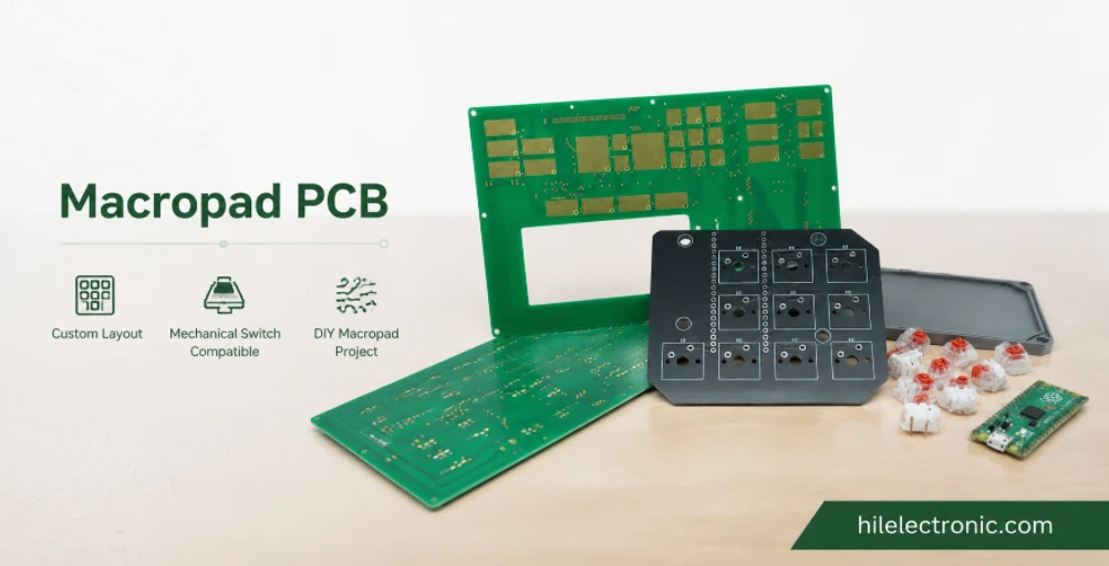
Macropad PCB Manufacturing & Custom PCBA
Table of contentsMacropad PCB Buying Guide and Quick...
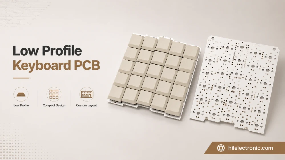
Low-Profile Keyboard PCB Manufacturing & Assembly
Table of contentsLow Profile and Choc Keyboard PCBA...
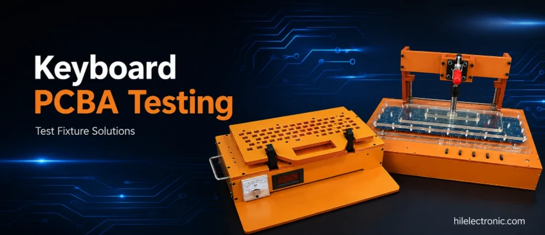
Keyboard PCBA Testing & Firmware Programming
Table of contentsKeyboard PCB Functional Testing Scope and...

Hall Effect Keyboard PCB Manufacturing & PCBA
Table of contentsHall Effect Keyboard PCB Buying...
How to get a quote for PCBs
Let us run DFM/DFA analysis for you and get back to you with a report.
You can upload your files securely through our website.
We require the following information in order to give you a quote:
-
- Gerber, ODB++, or .pcb, spec.
- BOM list if you require assembly
- Quantity
- Turn time
In addition to PCB manufacturing, we offer a comprehensive range of electronic services, including PCB design, PCBA (Printed Circuit Board Assembly), and turnkey solutions. Whether you need help with prototyping, design verification, component sourcing, or mass production, we provide end-to-end support to ensure your project’s success. For PCBA services, please provide your BOM (Bill of Materials) and any specific assembly instructions. We also offer DFM/DFA analysis to optimize your designs for manufacturability and assembly, ensuring a smooth production process.