
Copper Coin PCB Manufacturing Process: From Drilling to Coin Embedding

Introduction: Why Copper Coin PCB Manufacturing Requires Precision
High-power semiconductor modules demand efficient thermal dissipation pathways to maintain operational stability and prevent device failure. Copper coin PCB manufacturing addresses this requirement by integrating thick copper inserts directly into the substrate, creating localized thermal highways that outperform traditional thermal vias. This technology achieves thermal conductivity improvements exceeding 390 W/mK compared to standard PCB materials, with typical thermal resistance values below 0.5°C/W for power semiconductor applications.
The manufacturing process requires exceptional precision at every stage, from initial cavity formation through final embedding. Each step directly influences thermal performance and long-term reliability. This article examines the critical manufacturing stages that transform standard substrates into high-performance thermal management solutions.
Process Overview: Copper Coin PCB Manufacturing Workflow
The copper coin PCB manufacturing workflow follows six integrated stages that determine final thermal performance:
- Cavity design and drilling – Precision machining establishes foundation geometry with dimensional tolerances within ±20 μm for proper coin fitment.
- Copper coin machining and surface preparation – Material preparation ensures optimal thermal contact and mechanical adhesion characteristics at critical interfaces.
- Embedding and alignment – Precise positioning maintains thermal pathway integrity and prevents lateral displacement during subsequent processing.
- Resin filling and lamination – Controlled bonding manages thermal expansion mismatches while eliminating voids that compromise thermal conductivity.
- Surface flattening and planarization – Uniform topology enables consistent circuit layer formation across embedded coin regions.
- Thermal reliability and inspection – Comprehensive testing verifies performance parameters and structural integrity before deployment.
Process control across these stages determines whether the finished product meets demanding thermal and mechanical specifications for power electronics applications.
Cavity Drilling in Copper Coin PCB Manufacturing
Precision Machining Methods
Cavity formation establishes the geometric foundation for thermal performance in copper coin PCB manufacturing. CNC routing and laser machining achieve tolerances within ±20 μm, ensuring precise fit between cavity and copper insert. Dimensional deviation beyond this threshold creates gaps that compromise thermal contact and introduce resin voids during lamination.
Laser ablation offers superior edge definition for complex geometries but requires careful parameter optimization to prevent substrate charring. Mechanical routing provides faster throughput for simple cavity shapes while maintaining adequate precision for most power semiconductor applications.
Surface Quality Control
Cavity wall roughness directly impacts thermal conductivity and mechanical adhesion at the copper-substrate interface. Target roughness values range from 1.6 to 3.2 μm Ra to balance thermal contact with resin adhesion. Excessive smoothness reduces mechanical interlocking between resin and cavity walls, increasing delamination risk during thermal cycling.
Controlled roughness promotes resin wetting while maintaining continuous thermal pathways. Post-machining cleaning removes particulates that could create voids during the subsequent copper coin embedding process.

Copper Coin PCB Boards
Copper Coin Embedding Process: Critical Assembly Stage
Dimensional Matching and Fit Control
The copper coin embedding process requires precise dimensional matching between coin diameter and cavity opening. Interference fits ranging from 10 to 30 μm provide secure mechanical retention while avoiding substrate cracking during insertion. Press-fit methods apply controlled force to seat coins flush with the cavity floor without inducing substrate stress.
Automated vision systems verify alignment to within ±25 μm before lamination, preventing lateral displacement during resin flow. Misalignment creates asymmetric thermal pathways that degrade overall thermal resistance and generate localized hot spots in the final assembly.
Lamination Parameters in Copper Coin PCB Manufacturing
Successful copper coin PCB manufacturing depends on controlled lamination conditions that bond the assembly without warping:
- Temperature profile control – Ramp rates of 2-3°C per minute match thermal expansion coefficients between copper, resin, and substrate materials with peak temperatures from 170°C to 200°C.
- Applied pressure optimization – Force between 15 and 25 bar ensures complete resin flow around coin perimeters while preventing coin protrusion above the substrate surface.
- Vacuum-assisted processing – Removes trapped air that would create thermal resistance barriers at critical copper-substrate interfaces.
Surface Planarization in Copper Coin PCB Manufacturing
Resin Filling and Flow Management
Filling material selection balances thermal conductivity with processing characteristics during the copper coin embedding process. Thermally conductive epoxies containing ceramic fillers achieve 3-5 W/mK while maintaining sufficient flow during lamination. Pre-preg materials provide structural reinforcement but require careful resin content control to prevent starvation around coin edges.
Uniform resin distribution eliminates voids that compromise both thermal and dielectric performance. Controlled lamination pressure ensures consistent resin thickness between copper coin surface and adjacent substrate layers for optimal thermal transfer.
Planarity Achievement Methods
Post-lamination grinding removes excess copper and resin to achieve surface flatness within ±15 μm across the panel. Diamond abrasive wheels gradually reduce material while monitoring thickness with laser profilometry. Progressive grit reduction from 400 to 1200 mesh creates uniform surface topology suitable for photolithography.
Chemical-mechanical polishing provides final surface preparation, removing subsurface damage from mechanical grinding. Planarity verification before circuit imaging prevents registration errors and ensures consistent trace formation across regions containing embedded copper coins.

Copper Coin PCB
Reliability Testing in Copper Coin PCB Manufacturing
Thermal Performance Validation
Comprehensive testing validates copper coin PCB manufacturing quality through multiple thermal assessments:
- Thermal cycling evaluation – Testing between -40°C and 150°C for 1000 cycles reveals delamination tendencies and interface degradation under operational stress.
- Thermal resistance measurement – Direct measurement compares actual performance against design targets, verifying achievement of specified thermal conductivity values.
- Infrared thermography analysis – Identifies localized hot spots indicating incomplete thermal contact at coin-substrate interfaces requiring process adjustment.
- Heat shock testing – Extreme temperature gradients verify structural stability under rapid thermal transients encountered in power cycling applications.
Structural Integrity Analysis
Cross-sectional microscopy examines void formation, resin distribution, and interface quality throughout the copper coin embedding process regions. Shear testing applies lateral forces to quantify mechanical bond strength, targeting values above 10 MPa to prevent coin dislodgement during thermal stress. Microsectioning reveals resin penetration into cavity wall roughness and confirms complete filling around coin perimeters.
Highleap Electronics performs comprehensive reliability testing to ensure stable thermal and mechanical performance in copper coin PCBs across expected operational lifetimes.
Conclusion: Precision Manufacturing for High Thermal Reliability
Successful copper coin PCB manufacturing relies on tight process control from cavity machining to final reliability testing. High dimensional precision during drilling forms the foundation for accurate copper coin placement and efficient thermal transfer. Controlled embedding and lamination steps ensure proper bonding, minimized warpage, and consistent surface planarity for reliable circuit formation. Rigorous validation—through thermal cycling, cross-section inspection, and shear testing—confirms both mechanical integrity and long-term heat performance under demanding operating conditions.
At Highleap Electronics, our engineering team applies extensive manufacturing experience in copper coin PCB production and embedding process optimization. We integrate precision CNC machining, advanced lamination control, and in-house reliability testing to ensure every board meets the thermal and structural requirements of modern power semiconductor applications. This process-driven approach reflects our ongoing commitment to technical excellence, manufacturing reliability, and transparent quality assurance for our global customers.

Recommended Posts
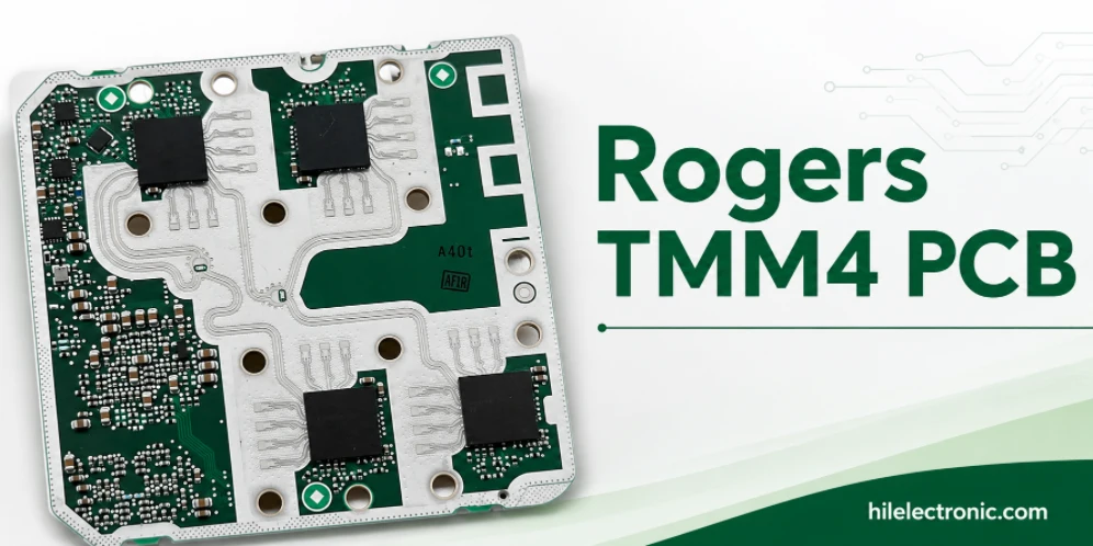
Rogers TMM4 PCB Manufacturer for Compact Microwave Filters
TMM4 is most useful when a microwave circuit must become...
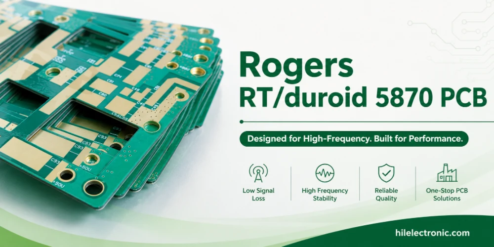
RT/duroid 5870 PCB Manufacturer for Low-Loss PTFE RF Circuits
RT/duroid 5870 is chosen when the RF path needs low loss,...
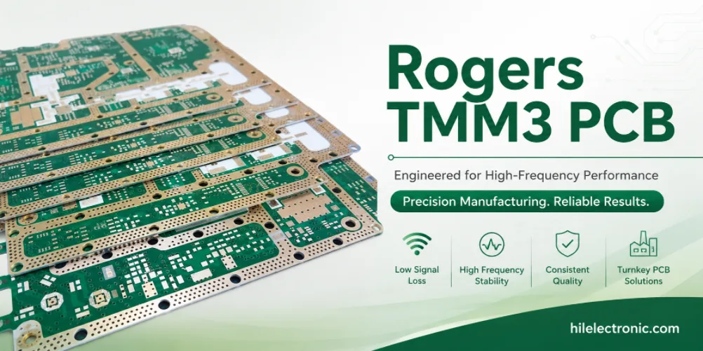
Rogers TMM3 PCB Manufacturer for Mechanical RF Modules
TMM3 is selected when an RF circuit must behave as part of...
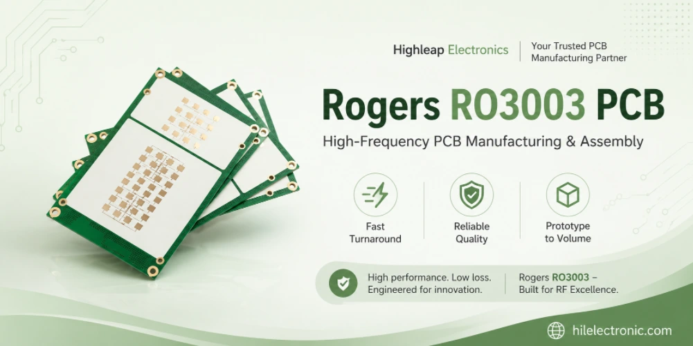
Rogers RO3003 PCB Manufacturer for Automotive Radar and mmWave Modules
A 77 GHz radar board is purchased as a working sensor...
How to get a quote for PCBs
Let‘s run DFM/DFA analysis for you and get back to you with a report. You can upload your files securely through our website. We require the following information in order to give you a quote:
-
- Gerber, ODB++, or .pcb, spec.
- BOM list if you require assembly
- Quantity
- Turn time
In addition to PCB manufacturing, we offer a comprehensive range of electronic services, including PCB design, PCBA, and turnkey solutions. Whether you need help with prototyping, design verification, component sourcing, or mass production, we provide end-to-end support to ensure your project’s success.
For PCBA services, please provide your BOM (Bill of Materials) and any specific assembly instructions. We also offer DFM/DFA analysis to optimize your designs for manufacturability and assembly, ensuring a smooth production process.