
Future Trends of Copper Coin PCBs in Advanced Packaging

The semiconductor industry is witnessing an accelerated shift toward advanced packaging architectures that demand higher thermal dissipation capacity and denser interconnect integration. As chip performance increases and form factors shrink, the boundary between conventional printed circuit boards and package substrates continues to blur.
Copper Coin PCBs emerge as a critical bridging technology that combines the manufacturability of traditional PCB processes with the thermal and electrical performance requirements of advanced packaging. This embedded substrate approach addresses the growing need for localized thermal management and high-current pathways in next-generation electronic systems.
Bridging the Gap Between PCB and Advanced Packaging with Copper Coin Technology
Traditional PCB fabrication and package substrate manufacturing have historically operated as distinct domains with different design rules and material systems. The convergence of these technologies is now driven by thermal challenges inherent in high-performance computing and power electronics. Copper Coin PCBs serve as an intermediate platform that integrates solid copper structures directly within dielectric layers, creating efficient thermal and electrical pathways that conventional plated through-holes cannot match.
Embedded Thermal Pathways for High-Power Modules
The copper coin structure functions as a localized heat spreader embedded within the PCB stackup. Unlike standard vias that rely on plated copper with limited cross-sectional area, embedded copper coins provide solid metal volumes that conduct heat vertically from active components to external heat sinks. This embedded substrate PCB approach proves effective in applications where power density exceeds the thermal management capability of conventional board designs.
Enabling Higher Integration Density
As advanced packaging pushes toward finer pitch interconnects and increased I/O counts, Copper Coin PCBs offer superior current-carrying capacity without compromising board real estate. The solid copper structure reduces electrical resistance and inductance compared to traditional via arrays, supporting high-frequency signal integrity requirements of modern packaging architectures.
From Power Electronics to Embedded Substrate Applications
The evolution of copper coin technology traces back to power module applications where IGBT and SiC devices generate substantial heat that must be efficiently removed. In these implementations, Copper Coin PCBs served as direct thermal interfaces between power semiconductors and cooling systems. The technology has since expanded into embedded substrate PCB designs for system-level integration.
Performance Advantages in Power Module Design
When compared to metal core PCBs or direct bonded copper substrates, copper coin technology offers distinct advantages in manufacturing flexibility and cost structure. While MCPCB provides excellent thermal performance through a continuous metal layer, it limits design freedom in routing and layer count. Copper Coin PCBs deliver targeted thermal management at specific locations while maintaining multilayer capability and routing density of conventional organic substrates. Modern power module architectures increasingly incorporate embedded copper coin structures to create low-impedance power distribution networks and enhanced thermal interfaces.
Integration of Copper Coin PCBs into 2.5D and 3D Packaging
The migration of copper coin technology into 2.5D and 3D packaging represents a significant expansion of the technology’s application scope. In these advanced architectures, Copper Coin PCBs function as vertical thermal vias that conduct heat through organic substrates while maintaining electrical isolation necessary for complex signal routing.
Thermal Management in HBM and AI Chip Packages
High bandwidth memory stacks and AI accelerators generate concentrated heat loads that challenge conventional package substrate designs. Embedded copper coin interconnects positioned strategically beneath memory dies or logic chips create direct thermal pathways to external cooling solutions. This approach proves valuable in 2.5D packaging configurations where silicon interposers provide horizontal connectivity but limited vertical thermal conduction.
Hybrid Substrate Architectures
Advanced packaging increasingly combines organic substrates with embedded copper structures to balance electrical performance, thermal management, and manufacturing cost. Copper Coin PCBs integrate seamlessly with fine-pitch redistribution layers and micro-bump technologies, enabling system architects to optimize thermal interfaces independently from electrical routing constraints. This hybrid approach allows designers to place copper coins precisely where thermal hotspots occur while maintaining signal integrity across the substrate.

Copper Coin PCB Cross Section
Material and Process Innovations for Fine-Pitch Copper Coin Integration
The advancement of Copper Coin PCBs into fine-pitch substrate applications requires continuous innovation in both materials and manufacturing processes. Achieving void-free embedding of copper structures within high-performance dielectric materials presents technical challenges that must be addressed to meet advanced packaging reliability standards.
Void-Free Embedding Process Development
The quality of copper coin bonding directly impacts thermal and electrical performance. Recent process developments focus on eliminating voids at the copper-dielectric interface through improved resin formulations and lamination parameters:
- Enhanced resin flow characteristics – Modified epoxy systems with controlled viscosity ensure complete wetting around copper structures during lamination cycles.
- Optimized lamination parameters – Precise temperature and pressure profiles eliminate trapped air and volatiles at bonding interfaces.
- Surface preparation protocols – Controlled oxide treatments on copper surfaces promote chemical adhesion with surrounding dielectric materials.
These advances enable copper coin technology to maintain consistent thermal conductivity across production volumes while supporting dimensional tolerances required for fine-pitch substrate designs.
High Flatness and Surface Planarity Control
Advanced packaging substrates demand exceptional surface planarity to enable thin-film lithography and micro-bump formation. Copper Coin PCBs embedding processes must control height variation across embedded structures to within micrometers, requiring precision grinding and polishing techniques adapted from semiconductor manufacturing. The integration of ceramic-filled resin systems offers enhanced thermal conductivity while maintaining electrical insulation properties necessary for multilayer substrate fabrication.
Reliability and Co-Design Challenges in Copper Coin PCBs
As copper coin technology transitions into advanced packaging applications, reliability considerations become increasingly critical. The embedded copper structures introduce material interfaces that must withstand thermal cycling, mechanical stress, and chemical exposure throughout the product lifecycle.
Thermal Cycling and Interface Integrity
The coefficient of thermal expansion mismatch between copper and surrounding organic materials generates stress at bonding interfaces during temperature excursions. Reliability testing for Copper Coin PCBs must validate interface integrity through accelerated thermal cycling that simulates operational conditions. Bonding integrity depends on both initial lamination process quality and long-term adhesion strength between dissimilar materials.
Warpage Control in Package Substrate Designs
Embedded copper structures influence overall warpage behavior of package substrates due to their high stiffness relative to organic dielectric layers. Design engineers must account for copper coin placement when modeling substrate deformation during assembly processes and thermal exposure. Key considerations include:
- Symmetric copper coin distribution – Balanced placement across substrate planes minimizes differential thermal expansion effects.
- Strategic stackup design – Alternating copper coin layers with compensating structures reduces cumulative warpage.
- Material selection optimization – Matching CTE values between copper coins and surrounding dielectrics reduces interfacial stress concentrations.
Successful implementation requires close collaboration between package designers and PCB manufacturers to optimize copper coin dimensions, placement, and bonding processes.
Future Outlook: Copper Coin PCBs in System-Level Integration
The role of Copper Coin PCBs continues expanding as the electronics industry pursues higher levels of system integration. System-in-package architectures that combine logic, memory, analog, and power management functions within single modules increasingly rely on embedded substrate technologies to manage thermal and electrical challenges.
Embedded Power Substrate Development
The integration of power delivery networks directly within package substrates represents a significant opportunity for copper coin technology. Embedded power substrates utilize thick copper structures to distribute high currents with minimal voltage drop while managing associated thermal dissipation. Copper Coin PCBs provide the structural foundation for these advanced power distribution architectures, enabling voltage regulator modules and power stages to be integrated at the package level.
High-Frequency and AI Computing Platforms
As computing platforms transition to higher operating frequencies and greater power densities, the thermal management capabilities of copper coin technology become increasingly valuable. AI accelerators and high-performance computing modules benefit from localized thermal pathways that embedded copper structures provide, enabling sustained performance under heavy computational loads. The technology convergence between PCB manufacturing and semiconductor packaging positions Copper Coin PCBs as a key enabler of next-generation system integration.
Conclusion: Expanding the Role of Copper Coin PCBs in Advanced Packaging
The evolution of Copper Coin PCBs from power module applications to advanced packaging substrates demonstrates the technology’s adaptability to increasingly demanding thermal and electrical requirements. As package-level integration continues advancing, embedded copper coin structures provide essential thermal management capability while maintaining compatibility with established PCB manufacturing processes.
Highleap Electronics supports next-generation packaging solutions through:
- Advanced copper coin embedding capabilities – Precision lamination processes ensure void-free bonding and consistent thermal performance across production volumes.
- Fine-pitch substrate expertise – Manufacturing capabilities supporting dimensional tolerances required for 2.5D and 3D packaging architectures.
- Design collaboration services – Early engagement with customers to optimize copper coin placement, material selection, and reliability validation.
- Integrated thermal management solutions – Combining embedded copper structures with high-performance dielectric materials for superior heat dissipation.
Our manufacturing expertise bridges traditional PCB fabrication with the precision requirements of advanced packaging substrates. Contact Highleap Electronics to discuss how copper coin technology can enhance thermal performance and reliability in your next-generation system designs.

Recommended Posts
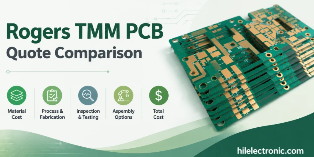
Rogers TMM PCB Quote Comparison and Cost Factors
Table of contentsCan Rogers TMM PCB Price Be Calculated...
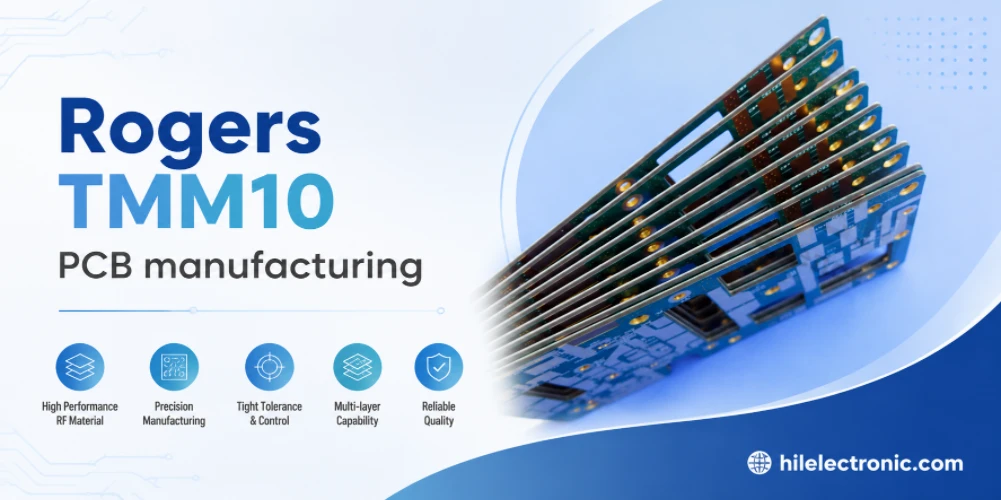
Rogers TMM10 PCB Manufacturing for RF Designs
Table of contentsHow TMM10 Shrinks RF StructuresTMM10 vs...
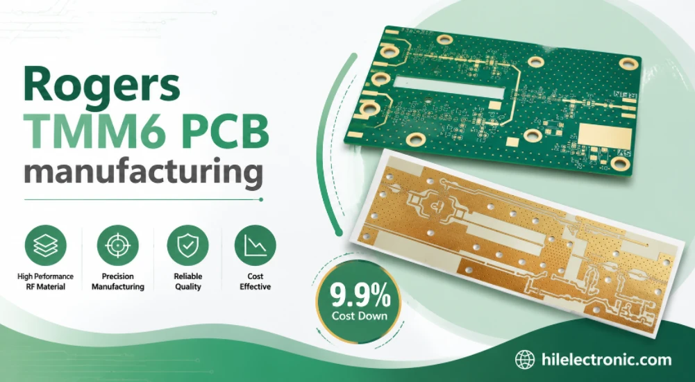
Rogers TMM6 PCB Manufacturing for Microwave Filters
Table of contentsWhy Microwave Filter Designers Use...
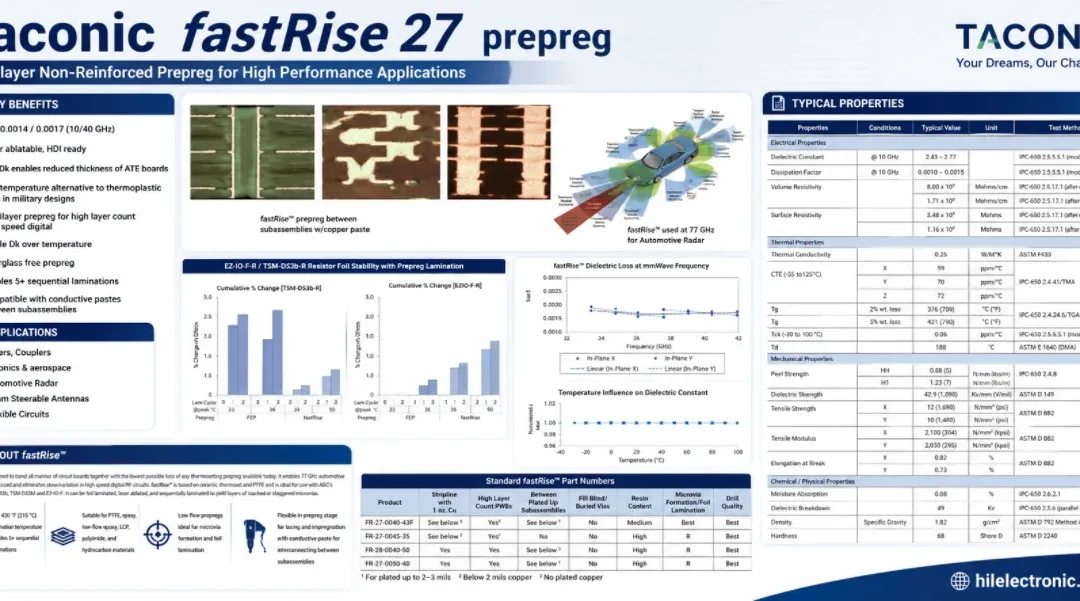
Taconic fastRise 27 Prepreg PCB Bonding and HDI Fabrication Service
Table of contentsWhat fastRise 27 Is—and What You Are...
How to get a quote for PCBs
Let‘s run DFM/DFA analysis for you and get back to you with a report. You can upload your files securely through our website. We require the following information in order to give you a quote:
-
- Gerber, ODB++, or .pcb, spec.
- BOM list if you require assembly
- Quantity
- Turn time
In addition to PCB manufacturing, we offer a comprehensive range of electronic services, including PCB design, PCBA, and turnkey solutions. Whether you need help with prototyping, design verification, component sourcing, or mass production, we provide end-to-end support to ensure your project’s success.
For PCBA services, please provide your BOM (Bill of Materials) and any specific assembly instructions. We also offer DFM/DFA analysis to optimize your designs for manufacturability and assembly, ensuring a smooth production process.