
DuPont Pyralux LF PCB Manufacturing for Flexible Circuit Projects
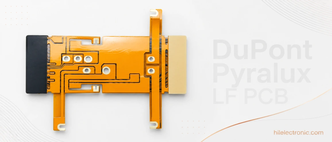
A Pyralux LF flex circuit should be quoted from its mechanical duty. A board that folds once during installation, a service loop that moves occasionally and a high-cycle dynamic flex cannot share one generic bend rule. DuPont’s current product information describes Pyralux LF as an acrylic-based family of copper-clad laminate, coverlay, bondply and sheet adhesive, with several polyimide, adhesive and copper constructions.
Highleap reviews the bend map, copper type, coverlay openings, stiffeners, rigid-flex transitions and assembly support before confirming the process. For severe dynamic-flex duty, the released construction and life test should be evaluated against suitable adhesiveless alternatives rather than assuming that a family name establishes bend life.
Choose Pyralux LF From the Required Flexing Mode
The phrase “flexible PCB” covers very different mechanical duties. An installation-flex circuit bends once during assembly and remains largely stationary. A limited-flex circuit may move during service or maintenance but not continuously. A dynamic-flex circuit experiences repeated cycles and must be designed around fatigue life. Pyralux LF can be used in a range of constructions, but the appropriate copper, dielectric, adhesive, coverlay and bend radius depend on which duty applies.
For a static harness replacement, design priorities may include thin profile, connector alignment and reliable folding into an enclosure. For a moving printhead, hinge, camera module or actuator, the neutral axis, conductor grain direction and repeated strain become dominant. The same layer count and outline can therefore require different stackups. Buyers seeking a custom flex PCB supplier should state the expected bend angle, radius, cycle count, temperature range and whether bending occurs during operation or only during installation.
| Flexing mode | Typical project question | Production information Highleap needs |
|---|---|---|
| Installation flex | Can the circuit be folded into the housing without permanent damage? | Final fold line, direction, forming fixture, bend radius and assembly sequence. |
| Limited service flex | Will maintenance movement overstress copper or plated features? | Expected cycles, connector forces, support points and minimum operating radius. |
| Dynamic flex | Can the conductor system survive repeated motion? | Cycle target, travel, frequency, temperature, copper selection and test method. |
| Rigid-flex transition | How is strain prevented at the rigid edge and coverlay termination? | Transition drawing, no-copper zones, coverlay overlap, adhesive details and stiffeners. |
Material names do not replace mechanical design. Review the available flexible PCB material constructions together with the movement requirement. Rolled-annealed copper is often evaluated for repeated bending, while electrodeposited copper may be acceptable in less demanding movement; the exact choice should follow the construction and supplier data rather than a universal rule.
Does a thinner circuit always last longer?
Lower thickness can reduce strain for a given bend radius, but a thin circuit can still fail if traces change direction in the bend, copper is unevenly distributed, plated holes sit near the flex line, or a stiffener ends abruptly. Very thin panels also require handling support during imaging, coverlay registration and assembly. The best construction is the thinnest one that still meets current, impedance, mechanical support and manufacturing requirements—not simply the minimum thickness a factory can produce.
Should components ever sit in the bend region?
Components, solder joints, plated holes and abrupt pad transitions should normally be kept away from active bending. When product geometry makes this difficult, the design needs local support, a revised bend line or a different mechanical concept. Highleap reviews the assembly drawing with the flex artwork because a board that is electrically correct can become unmanufacturable once a connector, shield or adhesive-backed stiffener is added.
Design the Bend Area Before the Stackup Is Released
A bend zone should be treated as a controlled mechanical feature. Conductors should run through it with smooth geometry and without unnecessary width changes. Corners, neck-downs and teardrop transitions require attention because local stress concentrates where the copper cross-section changes. Copper balance on opposing sides also matters: an asymmetric circuit can curl during processing or shift the neutral axis away from the intended position.
Coverlay openings need enough registration allowance for fabrication without exposing unsupported conductor edges. Stiffeners should support connectors and solder joints, but their edges must not create a knife-edge bend. Adhesive flow must be considered around fine-pitch pads and openings. In rigid-flex products, the transition from rigid stackup to flexible layers must be defined in the mechanical data rather than inferred from layer artwork.
How close can a plated feature be to the bend?
There is no single universal distance because the answer depends on thickness, copper, bend radius, layer count and movement. The drawing should identify the bend line and keep-out region so the fabricator can review the actual geometry. If a via, slot or connector lands close to the transition, Highleap may recommend moving the feature, extending a stiffener or changing the outline. This is a design-for-reliability decision, not a sales preference.
For combined rigid and flexible structures, use a detailed rigid-flex PCB design review rather than relying on an ordinary multilayer note. The release should distinguish flex copper from rigid copper, identify coverlay and solder-mask boundaries, define no-flow or bonding materials if used, and show the final forming condition.
- Mark every bend line, direction, angle and minimum radius on the mechanical drawing.
- Identify whether the bend is formed once, moved occasionally or cycled during operation.
- Keep plated holes, component pads and abrupt conductor changes outside the active bend where possible.
- Define copper type, copper thickness, dielectric, adhesive and coverlay by construction.
- Show stiffener material, thickness, adhesive, outline and distance from the bend.
- State any life-cycle test or customer-specific mechanical acceptance requirement.
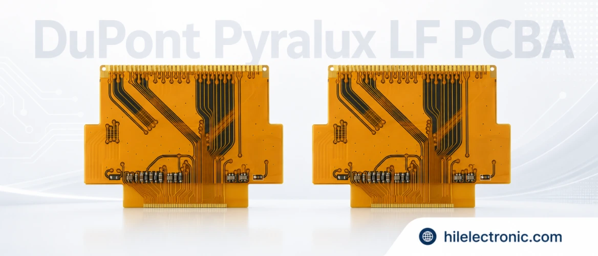
Why Pyralux LF Flexible Circuits Fail During Fabrication
Flexible materials move during etching, lamination and thermal processing. Artwork compensation must be based on the actual construction and panel route. Fine traces on thin polyimide can distort if the panel is unsupported. Coverlay can shift or wrinkle. Adhesive can flow into openings. Copper can be over-etched at narrow necks. Stiffeners can be misregistered. Each risk is manageable, but only if the factory knows which dimensions are critical to function.
Highleap uses CAM review to compare copper geometry with coverlay, outline, stiffener and assembly data. Tooling is planned to limit panel movement. Inspection focuses on coverlay registration, conductor width, opening size, stiffener placement and surface condition. Where a dynamic bend requirement is important, a first-article lot may include dedicated test coupons or formed samples agreed with the customer.
Coverlay alignment and adhesive flow
Coverlay is not equivalent to liquid solder mask. It is a film construction with an adhesive system and its own dimensional behaviour. Openings must be sized for registration and final pad access. Too little allowance can cover a pad; too much can leave unsupported copper or reduce insulation. Adhesive squeeze-out near fine-pitch lands can interfere with assembly. These details should be checked before tooling, particularly on compact connector areas.
Etching thin copper without damaging fatigue life
Fine-line flexible PCB fabrication requires stable imaging and etch control. Excessive undercut changes trace width and can create weak sections. Sharp trace corners or poorly shaped transitions can concentrate stress. Highleap can apply manufacturing compensation, but the design owner should approve any change that alters controlled impedance, current capacity or critical geometry.
Rigid-flex transitions and local delamination
The rigid edge concentrates strain when the product is folded. Coverlay overlap, adhesive placement, copper routing and the location of plated holes all affect the result. The rigid and flex materials also move differently during lamination. A trial construction may be appropriate for unusual thickness, asymmetric copper or tight transition geometry. Quick-turn service is useful only after this risk is understood; an unrealistic schedule can create more rework than it saves.
When schedule matters, a fast-turn rigid-flex PCB plan should identify material stock, tooling, coupon requirements and assembly fixtures before the promised ship date is accepted.
Assembly Rules for Components, Connectors and Stiffeners
Flexible circuit assembly needs mechanical support. Thin panels can move under stencil pressure, pick-and-place acceleration or reflow airflow. A carrier fixture may be required to keep the panel flat. Stiffeners must support connectors, BGA or fine-pitch components without shifting the bend region. The reflow profile must suit the component mix, surface finish, adhesive system and moisture condition.
Highleap can provide flex PCB assembly together with board fabrication. Combining the work allows the panel format, tooling holes, breakaway support and stiffener locations to be designed for the assembly line rather than added after the bare boards are finished. The BOM and centroid data should be supplied early enough to review component clearance and polarity.
Connector areas need more than a stiffener callout
A connector can apply insertion, extraction and cable loads. The stiffener material, adhesive, thickness and outline should be selected for that load, while the copper transition should avoid abrupt stress concentration. Gold fingers or contact areas may require controlled thickness and bevel details. If the connector is hand-inserted after shipment, the customer should define the final process so packaging and handling do not pre-form the circuit incorrectly.
First-article inspection should include mechanics
Electrical test confirms continuity and isolation, but it does not prove that a coverlay opening, stiffener edge or fold line is correct. A flexible PCB first article can include dimensional inspection, formed-sample review, assembly fit, visual criteria and photographs. Use a defined first-article inspection plan where mechanical alignment is critical.
What Highleap Needs to Quote a Pyralux LF PCB
The quotation package should show the final product, not only the copper artwork. Include the flex or rigid-flex stackup, material and copper requirement, coverlay, stiffeners, bend information, surface finish, quantities, panel preference and acceptance criteria. For assembly, include the BOM, centroid, assembly drawing, programming and test information, plus any fixtures supplied by the customer.
- Gerber or ODB++ layers with clear flex, rigid and coverlay identification;
- mechanical drawing with bend lines, final formed shape and stiffener details;
- material construction, copper type and finished thickness requirements;
- controlled impedance or current requirements where applicable;
- prototype, low-volume and forecast production quantities;
- BOM, pick-and-place, assembly drawings, test specification and packaging needs.
Special materials and coverlay constructions must be checked for stock before a quick-turn date is confirmed. Payment terms, currency and shipping method are stated in the quotation. Small orders can use international express; larger production can use agreed freight options. After delivery, Highleap keeps project and lot records so engineering questions can be investigated against the approved files and inspection data.
Panelisation must support both fabrication and assembly
A flex circuit panel needs temporary rigidity without creating damage during depanelisation. Tooling holes, rails, tabs and local support should be positioned so the panel remains stable through coverlay, surface finish, printing and placement. The panel must also release without tearing the flex outline or placing stress on fine conductors. Highleap can propose a fabrication-and-assembly panel after reviewing the component and connector layout.
For very small circuits, arrays may improve handling and cost, but the customer should approve the method used to separate units. Routing, laser cutting, punching and tab designs create different edge conditions. A circuit that folds close to the outline may require special attention so edge damage does not become a crack initiation point.
Surface finish should follow the contact and assembly requirement
Flexible circuits may include solder pads, connector contacts, wire-bond areas or exposed copper. Each use can require a different finish or thickness control. The drawing should identify hard-gold contact areas, solderable pads and any regions that must remain free of coating. Open substitution between finishes can affect soldering, contact wear, thickness and bend behaviour.
Highleap reviews the finish together with coverlay openings and stiffeners. On fine-pitch areas, finish thickness and pad definition can affect solder paste and component placement. On connector fingers, bevel, stiffener thickness and final overall thickness must work together. These details are included in the quotation instead of being resolved after boards are complete.
Electrical test does not validate bend life
Every production panel can be electrically tested for continuity and isolation, but bend performance requires a representative mechanical test. If the product has a quantified cycle requirement, the customer should provide the bend radius, motion, speed, temperature and failure criterion. A simple hand fold is not equivalent to a controlled dynamic-flex test.
For high-risk projects, Highleap can fabricate coupons using the same copper and layer construction. The customer can test them in the product environment or define an external qualification method. Once approved, the construction, copper and artwork should remain controlled for repeat orders.
Packaging and shipping matter for formed flex circuits
Thin circuits can crease, curl or collect contamination during transport. The delivery format should state whether units are shipped flat, in panels, with temporary stiffening, or in a formed condition. Trays, antistatic bags, separators and moisture protection are selected according to the assembly and surface finish. Shipping a flex circuit in the wrong orientation can damage it before the customer opens the package.
Highleap confirms packaging and international transport with the order. Prototypes often use express courier service; production may use agreed freight. If the customer will store the circuits before assembly, shelf-life and storage instructions should accompany the shipment where required.
How field issues are investigated
A crack reported after installation can result from design radius, assembly forming, connector load, copper construction or fabrication. Highleap reviews the returned sample, lot record, approved drawing and assembly information. Clear bend-zone and acceptance requirements make this investigation much faster. After-sales support is strongest when the original order captured the product’s mechanical duty instead of treating the board as a flat electrical item.
Material note: Pyralux LF is a family of flexible laminate and related material constructions. The exact DuPont product, copper, adhesive, coverlay and processing guidance must be frozen for production; the family name alone is not a complete stackup.

Recommended Posts

TMM4 Filter PCB Manufacturing
TMM4 filter PCB manufacturing is controlled by the...

TMM3 PCB Manufacturing for RF Modules
TMM3 PCB manufacturing is most useful where the RF module...

TMM6 PCB Fabrication
TMM6 fabrication is the process-control page for a mid-Dk...

TMM10 PCB Manufacturing for Compact RF Designs
Table of contentsHow TMM10 Shrinks RF StructuresTMM10 vs...
How to get a quote for PCBs
Let’s run DFM/DFA analysis for you and get back to you with a report. You can upload your files securely through our website. We require the following information in order to give you a quote:
-
- Gerber, ODB++, or .pcb, spec.
- BOM list if you require assembly
- Quantity
- Turn time
For PCBA services, please provide your BOM (Bill of Materials) and any specific assembly instructions. We also offer DFM/DFA analysis to optimize your designs for manufacturability and assembly, ensuring a smooth production process.