
HDI PCB Reliability: Understanding Failure Modes and Prevention Strategies

Introduction: Why HDI PCB Reliability Matters
High Density Interconnect printed circuit boards have become essential for modern electronics requiring miniaturization and enhanced performance. These advanced boards support increasingly complex device architectures through fine-line traces, stacked microvias, and multi-layer constructions. However, sophisticated manufacturing processes and demanding operational environments create specific challenges that can compromise HDI PCB reliability and product longevity.
The complexity stems from interactions between dense microvia structures, thin dielectric layers, and thermal stress during manufacturing and field operation. Understanding these failure mechanisms becomes critical for aerospace, automotive electronics, and telecommunications infrastructure where system failures carry significant consequences. This analysis examines primary reliability concerns and presents practical strategies for enhancing long-term performance.
Common HDI PCB Reliability Failure Modes
Microvia Cracking and Failure
Microvia failure represents one of the most prevalent concerns in HDI PCB reliability. The thermal expansion mismatch between copper and resin materials creates mechanical stress at the via barrel interface, particularly during thermal cycling between -55°C to 125°C. Laser drilling processes introduce additional stress concentrations through heat-affected zones that weaken copper adhesion.
Incomplete copper filling within the microvia structure exacerbates the problem by creating void spaces that concentrate mechanical strain. The manifestation typically appears as intermittent signal failures or complete open circuits between layers. Scanning electron microscopy frequently reveals circumferential cracks at the via-pad interface or longitudinal fractures through the copper barrel itself.
Copper Migration and Electrochemical Migration
Moisture ingress combined with electrical bias creates conditions for metallic ion transport between adjacent conductors. This electrochemical migration process gradually forms conductive pathways that bridge insulating gaps, leading to short circuits or leakage currents. The phenomenon accelerates under elevated temperature and humidity conditions, particularly affecting HDI PCB reliability in harsh environments.
Standard qualification testing employs Highly Accelerated Stress Testing (HAST) at 130°C/85%RH or 85°C/85%RH exposure to evaluate susceptibility. The combination of electric field strength, moisture content, and ionic contamination determines dendrite formation rate, directly impacting long-term reliability performance.
Conductive Anodic Filament (CAF) Growth
CAF formation occurs through electrochemical degradation at the glass-resin interface within the dielectric material. When moisture penetrates the laminate structure, it creates an electrolytic path along fiber bundles between conductors at different potentials. The resulting dendritic growth follows glass fiber orientation, eventually creating low-resistance paths that cause catastrophic failures.
CAF prevention requires careful attention to material selection and processing parameters. The interface quality between glass reinforcement and resin matrix directly influences vulnerability to filament growth. Modern laminate systems incorporate improved sizing treatments and resin formulations specifically designed to enhance HDI PCB reliability against this failure mechanism.
Delamination and Resin Cracks
Thermal stress during lamination or assembly reflow cycles can exceed adhesive strength between copper and dielectric layers. This stress concentration leads to delamination, manifesting as visible separation or blister formation within the layer stackup. The problem intensifies with increased layer count and incompatible thermal expansion properties.
Resin cracking frequently accompanies delamination as a secondary effect of thermal stress. These cracks provide pathways for moisture ingress, which further degrades dielectric properties and accelerates other failure mechanisms. The interconnected nature of these degradation processes makes delamination particularly problematic for sustained HDI PCB reliability.

Root Causes Affecting HDI PCB Reliability
Material Property Mismatches
The coefficient of thermal expansion (CTE) difference between copper conductors, dielectric layers, and microvia fill materials creates thermomechanical stress during temperature excursions. This CTE mismatch becomes more pronounced in HDI configurations due to higher density of vertical interconnections and thinner dielectric layers between copper planes.
Typical CTE values demonstrate the challenge:
- Copper foil: 17 ppm/°C in-plane
- FR-4 dielectric: 14-17 ppm/°C in-plane, 50-70 ppm/°C through-thickness
- Filled microvia copper: 16-18 ppm/°C
Laser Drilling Process Impact
Laser drilling introduces heat-affected zones surrounding the microvia that can damage resin structure and create weakened interfaces for subsequent copper deposition. The thermal energy required to ablate dielectric material typically reaches 1000-2000°C instantaneously. Optimization of laser parameters balances drilling efficiency against material degradation to maintain microvia reliability over operational lifetime.
Copper Filling Quality
The quality of electrolytic copper filling within microvias significantly impacts structural integrity of vertical connections. Incomplete filling creates void spaces that concentrate stress and reduce current-carrying capacity. Copper plating chemistry, current density profiles (typically 15-30 ASF), and geometric via design all influence final fill quality and overall HDI PCB reliability.
Moisture Absorption Characteristics
Moisture absorption of dielectric materials fundamentally affects insulation reliability. Higher moisture content reduces insulation resistance, accelerates copper migration, and increases CAF susceptibility. Standard FR-4 absorbs 0.10-0.15% moisture by weight, while advanced low-moisture materials achieve below 0.05%. Material selection must balance electrical performance against hygroscopic properties for adequate reliability in intended operating environments.
HDI PCB Reliability Testing Methods
Thermal Cycling Testing
Thermal cycling subjects assemblies to repeated temperature extremes to simulate operational stress and verify HDI PCB reliability. Standard test conditions include -55°C to 125°C cycling with 15-minute dwell times at each extreme. This accelerated test reveals microvia fatigue, solder joint degradation, and laminate stress failures within compressed timeframes.
The number of cycles to failure provides quantitative data for reliability predictions. High-reliability applications typically require 500-1000 cycles minimum, while automotive and aerospace applications may demand 2000 cycles or more to meet qualification standards.
Highly Accelerated Stress Testing (HAST)
HAST combines elevated temperature, humidity, and electrical bias to evaluate susceptibility to electrochemical migration and CAF formation. Standard conditions of 130°C and 85% relative humidity with 3-50V applied bias create worst-case scenarios for these failure mechanisms. Insulation resistance monitoring during 96-500 hour exposure tracks degradation progression and identifies design weaknesses affecting HDI PCB reliability.
Cross-Sectional Microsection Analysis
Cross-sectional analysis through microsectioning provides direct observation of internal HDI structures. This destructive testing method reveals copper fill quality within microvias, interface adhesion between layers, and presence of defects such as voids or cracks. Systematic sectioning at critical locations guided by IPC-TM-650 Method 2.1.1 ensures representative sampling of construction quality.
Surface Insulation Resistance (SIR) Testing
SIR testing evaluates ionic contamination levels that can compromise HDI PCB reliability. The test measures leakage current between closely-spaced conductors (typically 0.5mm spacing) under 85°C/85%RH conditions with 50V bias applied. Results indicate effectiveness of cleaning processes and identify potential electrochemical migration risks. Compliance with IPC-6016 Class 3 standards requires minimum SIR of 100 megohms after 168 hours exposure.

Strategies for Improving HDI PCB Reliability
Design Phase Optimization
Design-phase considerations significantly influence ultimate reliability outcomes. Controlling microvia aspect ratios below 1:1 for laser-drilled vias reduces stress concentrations and improves copper fill quality. Thoughtful stackup design using materials with compatible thermal expansion properties minimizes thermomechanical stress during thermal cycling.
Key design parameters for enhanced reliability:
- Microvia aspect ratio: Maximum 1:1 for optimal reliability
- Via capture pad: Minimum 150μm diameter for 100μm laser via
- Spacing from via to adjacent features: Minimum 150μm to reduce stress concentration
- Layer-to-layer registration tolerance: ±75μm for stacked via structures
Material Selection for Enhanced Reliability
High glass transition temperature (Tg) laminates maintain dimensional stability at elevated processing and operating temperatures. Materials with Tg above 170°C provide adequate margin for lead-free reflow processing at 260°C peak temperature. Low moisture absorption resin systems (below 0.05% water uptake) reduce susceptibility to electrochemical migration and CAF growth, directly improving HDI PCB reliability.
Advanced laminate materials specifically formulated for HDI applications include modified epoxy systems, polyimide constructions, and low-Dk/Df materials. Selection depends on balancing electrical performance requirements against thermal and mechanical reliability needs for the specific application environment.
Manufacturing Process Control
Laser drilling parameter development minimizes heat-affected zones while maintaining geometric accuracy. Typical UV laser settings include pulse frequencies of 30-80 kHz with energy levels of 10-30 μJ per pulse. Copper plating processes require careful control of chemistry composition, temperature (typically 22-28°C), and current density to achieve complete via filling without excessive internal stress.
Surface preparation techniques ensure adequate adhesion between layers and prevent delamination. Oxide alternative treatments or mechanical scrubbing followed by desmear processing creates appropriate surface texture for reliable copper-to-resin bonding, essential for long-term HDI PCB reliability.
Assembly and Testing Procedures
Reflow profile optimization balances peak temperature requirements against thermal stress on microvia structures. Recommended profiles for HDI assemblies limit peak temperature to 245-250°C (compared to 260°C for standard boards) and reduce time above liquidus to minimize thermal exposure. Ramp rates should not exceed 2-3°C per second to control thermal gradient stress.
Cleaning processes must effectively remove flux residues without damaging fine-pitch features or introducing moisture into the laminate. No-clean flux chemistry or carefully controlled aqueous cleaning with thorough drying cycles maintains HDI PCB reliability standards.
Case Studies of HDI Reliability Performance
Automotive ECU Application
Automotive electronic control unit applications demonstrate the importance of microvia reliability under thermal cycling conditions. Testing programs for these safety-critical systems revealed that optimized laser drilling parameters combined with controlled copper plating reduced microvia cracking rates by more than 60 percent. The improvements enabled qualification to 2000 thermal cycles from -40°C to 125°C, meeting AEC-Q100 Grade 1 automotive reliability requirements.
Statistical analysis showed mean cycles to failure increased from 1200 to over 3000 cycles with process optimization. This performance enhancement directly translated to improved field reliability and reduced warranty costs for automotive OEM customers.
Telecommunications Infrastructure
Communication infrastructure equipment operating in outdoor environments faces challenges from combined temperature and humidity exposure. Accelerated testing at 85°C/85%RH identified CAF growth as a primary concern for HDI boards in these applications, with initial designs showing insulation resistance degradation below acceptable thresholds within 500 hours exposure.
Implementation of improved laminate materials with enhanced glass-resin interface stability extended mean time to failure by a factor of three. Modified resin formulations and optimized curing cycles achieved over 1500 hours HAST exposure without CAF formation, enabling warranty commitments for 15-year field deployment while maintaining HDI PCB reliability standards.
Conclusion: Achieving Superior HDI PCB Reliability
HDI PCB reliability emerges from the complex interaction between design decisions, material properties, and manufacturing processes. The critical failure modes of microvia cracking, copper migration, CAF growth, and delamination each respond to specific control measures implemented throughout the product lifecycle. Understanding these mechanisms enables engineers to make informed tradeoffs between performance requirements and reliability objectives.
Microvia structures, thermal property management, and moisture control represent the primary levers for improving long-term reliability. Systematic qualification testing using industry-standard protocols provides confidence in design robustness before committing to production.
Highleap Electronics delivers proven HDI PCB reliability through:
- Advanced microvia process control with laser drilling optimization and controlled copper fill plating to minimize cracking and ensure structural integrity
- Comprehensive reliability testing programs including thermal cycling, HAST, and microsection analysis aligned with IPC-TM-650 and IPC-6016 standards
- Material qualification systems featuring high-Tg laminates and low-moisture resin systems specifically selected for demanding applications
- Statistical process control monitoring critical parameters affecting long-term reliability performance throughout manufacturing
Partner with Highleap Electronics for HDI PCB manufacturing and assembly backed by rigorous quality systems and reliability engineering expertise. Contact our engineering team to discuss your high-reliability application requirements and receive detailed design-for-reliability recommendations tailored to your specific performance objectives.

Recommended Posts
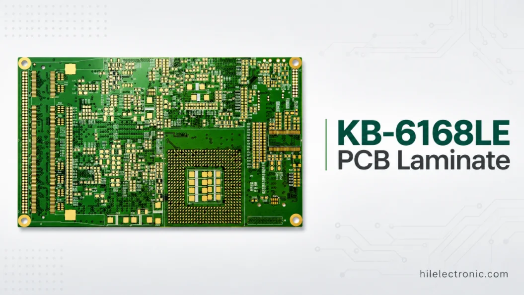
KB-6168LE PCB Laminate for Low Z-CTE Multilayer PCB Manufacturing
KB-6168LE PCB laminate is a Kingboard high-Tg, anti-CAF,...
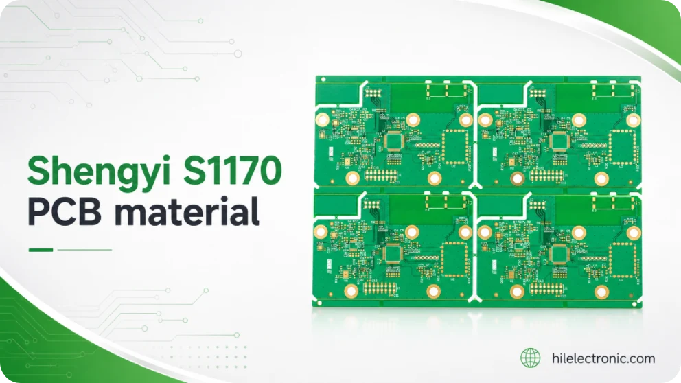
Shengyi S1170 PCB Material for High-Tg Lead-Free Multilayer PCB Manufacturing
Shengyi S1170 PCB material is a lead-free compatible,...

NP-175F PCB Laminate for High-Reliability Multilayer Boards
NP-175F PCB laminate is a Nan Ya high-Tg, filled...

High CTI FR-4 PCB Manufacturing for Insulation-Critical Boards
High CTI FR-4 is used when a PCB design needs stronger...
How to get a quote for PCBs
Let‘s run DFM/DFA analysis for you and get back to you with a report. You can upload your files securely through our website. We require the following information in order to give you a quote:
-
- Gerber, ODB++, or .pcb, spec.
- BOM list if you require assembly
- Quantity
- Turn time
In addition to PCB manufacturing, we offer a comprehensive range of electronic services, including PCB design, PCBA, and turnkey solutions. Whether you need help with prototyping, design verification, component sourcing, or mass production, we provide end-to-end support to ensure your project’s success.
For PCBA services, please provide your BOM (Bill of Materials) and any specific assembly instructions. We also offer DFM/DFA analysis to optimize your designs for manufacturability and assembly, ensuring a smooth production process.