
HDI PCB in Medical Devices: Enabling Precision and Miniaturization

Introduction – Why Medical HDI PCB Technology Matters
The medical electronics industry demands smaller, smarter, and more reliable devices that improve patient outcomes while reducing invasiveness. This evolution requires circuit boards capable of supporting high component density, maintaining signal integrity in compact spaces, and delivering unwavering reliability over extended operational lifespans. Medical HDI PCB technology addresses these requirements through high-density interconnections, precisely controlled impedance paths, and optimized spatial efficiency.
The integration of miniaturized PCB for medical devices has become essential. As diagnostic equipment becomes portable, wearable monitors shrink to patch-sized form factors, and implantable devices require biocompatible housings, the underlying circuit architecture must support increasingly complex functionality within diminishing physical envelopes.
Core Design Requirements of Medical HDI PCB
Medical electronic applications impose unique constraints that distinguish them from consumer or industrial circuit board requirements. Medical HDI PCBs must demonstrate zero-defect performance across years of continuous operation, often in challenging physiological environments where temperature fluctuations, humidity exposure, and mechanical stress occur regularly.
Critical Performance Parameters
Engineers working with miniaturized PCB for medical devices face distinct challenges:
- High reliability and long-term stability – Medical environments demand zero-failure performance with operational lifetimes measured in years or decades.
- Compact design and lightweight construction – Essential for wearable biosensors and implantable therapeutic devices constrained by anatomical limitations.
- Signal integrity and low noise performance – Medical devices frequently measure microvolt-level biological signals with precision requirements in parts per million.
- Biocompatibility and material safety – Substrate materials, surface finishes, and conformal coatings must meet stringent regulatory standards for cytotoxicity and long-term stability.
Why HDI PCBs Are Ideal for Medical Devices
Miniaturization Capabilities
HDI PCB technology enables component densities that conventional designs cannot support through microvias, fine-line traces, and advanced build-up structures. The technology supports component pitches below 0.4mm, via diameters under 0.15mm, and trace widths approaching 50 microns, facilitating three-dimensional circuit architectures that maximize functional density per unit area.
Medical applications benefit directly from this miniaturization potential. Glucose monitoring systems achieve wearable form factors while incorporating radiofrequency communication, precision analog measurement, and microcontroller functionality. Cardiac pacemakers and neurostimulators utilize HDI structures to house therapeutic pulse generators, telemetry systems, and power management circuits within titanium cases measuring less than 50 cubic centimeters.
Enhanced Electrical Performance
The electrical advantages of medical HDI PCB designs stem from reduced interconnection lengths and optimized signal path geometries. Shorter trace runs between components decrease propagation delays, minimize parasitic inductance and capacitance, and reduce susceptibility to electromagnetic interference.
High-definition imaging modules for ultrasound systems, endoscopic cameras, and optical coherence tomography equipment rely on HDI PCB structures to maintain signal fidelity across multiple parallel data channels. The technology supports controlled impedance routing, differential pair management, and ground plane optimization techniques that preserve signal integrity even as data rates increase and circuit densities intensify.
Improved Reliability Through Design
Laser-drilled microvias and thin dielectric layers characteristic of HDI construction reduce mechanical stress concentrations that contribute to solder joint failures in conventional through-hole designs. Sequential lamination build-up processes distribute stress across multiple layers rather than concentrating mechanical loads at discrete through-hole locations.
For implantable medical devices requiring decades of operational life, these reliability improvements translate directly into enhanced patient safety and reduced revision surgery rates. The design flexibility inherent in medical HDI PCB architectures accommodates complex signal routing requirements while maintaining structural integrity necessary for long-term reliability.

Medical Electronics
Material and Stackup Considerations for Medical HDI PCB
Medical-Grade Substrate Selection
Substrate material selection for medical HDI PCBs balances electrical performance requirements against biocompatibility constraints and mechanical stability needs. Standard FR-4 materials suffice for many external medical devices, while high-reliability applications may specify polyimide substrates or specialized low-loss laminates such as Rogers 4000 series materials.
The selection of biocompatible PCB materials becomes critical for implantable devices or applications involving direct patient contact. Materials must withstand sterilization processes including autoclave cycles, ethylene oxide exposure, or gamma irradiation without degradation of electrical properties or outgassing of potentially harmful compounds.
Optimized Layer Stackup Architecture
Medical HDI PCB designs typically employ 2+N+2 or 3+N+3 build-up structures, where N represents the core layer count. This architecture provides dedicated signal routing layers while maintaining controlled impedance environments and robust power distribution networks.
Dielectric layer thickness selection influences both electrical performance and manufacturing reliability. Medical applications often specify slightly thicker dielectrics than consumer electronics to enhance reliability margins, accepting modest electrical performance tradeoffs in exchange for improved long-term stability.
Thermal Management Integration
Medical devices operating in contact with human tissue face strict thermal limitations to prevent patient injury. HDI PCB designs for medical electronics must incorporate thermal management features including dedicated thermal vias, copper pour regions for heat spreading, and strategic component placement to minimize hot spots.
Reliability and Testing in Medical-Grade HDI Boards
Industry Standards and Classification
Medical HDI PCBs conform to IPC-6012 Class 3 or Class 3A specifications, representing the highest reliability levels defined by industry standards. These classifications mandate reduced tolerances on conductor spacing, increased minimum copper thickness in holes, and enhanced process controls compared to consumer electronics applications.
Microvia reliability testing forms a critical component of medical HDI PCB qualification. Cross-sectional analysis verifies barrel copper thickness uniformity, absence of voids or discontinuities, and proper resin fill in stacked via structures. Conductive anodic filament testing evaluates the board’s resistance to electrochemical migration failures under humidity and voltage stress.
Environmental Stress Validation
Medical-grade HDI PCBs undergo accelerated life testing that subjects boards to temperature cycling between extremes exceeding anticipated service conditions, humidity exposure at elevated temperatures, and mechanical shock representative of shipping and handling stresses.
Traceability and process control documentation requirements for medical HDI PCB manufacturing exceed those of most other industries. Each production lot requires detailed records of material certifications, process parameters at every manufacturing step, and inspection results traceable to individual boards or panels.

Common Applications of Medical HDI PCBs
Implantable Medical Devices
HDI PCB for pacemakers and neurostimulators represents the most demanding application of miniaturized PCB technology in medical electronics. These devices require extreme reliability over operational lifetimes measured in years or decades while occupying volumes constrained by anatomical limitations.
The circuit boards support complex functionality including therapeutic pulse generation, sensing amplifiers, wireless telemetry, and power management, all while maintaining biocompatibility and hermeticity within sealed enclosures. Implantable drug delivery systems, cochlear implants, and deep brain stimulation devices similarly rely on HDI PCB technology to achieve necessary component density.
Diagnostic Imaging Equipment
Miniaturized HDI PCBs in ultrasound systems enable probe designs with increased channel counts and enhanced beamforming capabilities while reducing probe diameter and weight. The circuit boards route high-frequency signals from transducer arrays to processing electronics while maintaining impedance control and minimizing crosstalk between channels.
Computed tomography and magnetic resonance imaging systems utilize HDI PCBs in detector arrays, gradient coil drivers, and signal processing modules where space constraints and electromagnetic compatibility requirements demand advanced interconnection technology.
Wearable Health Monitors
HDI PCB in ECG patches and glucose monitors enables the form factors that make continuous physiological monitoring practical for outpatient and home care applications. These devices integrate sensing electrodes, analog signal conditioning, analog-to-digital conversion, microcontroller processing, and wireless data transmission within patches measuring centimeters in diameter.
Continuous glucose monitors exemplify the integration challenges addressed by medical HDI PCB technology. The devices combine electrochemical sensors requiring precision analog measurement, calibration algorithms executing on embedded processors, and Bluetooth Low Energy transceivers for smartphone connectivity.
Surgical and Robotic Instruments
Rigid-flex HDI PCB for robotic surgical systems provides three-dimensional circuit routing necessary for articulated instrument mechanisms while maintaining reliability under repeated flexure cycles. The combination of rigid sections housing component assemblies and flexible interconnections accommodating mechanical motion enables instrument designs impractical with discrete cable assemblies.
Minimally invasive surgical instruments increasingly incorporate sophisticated electronics including force sensors, position encoders, tissue impedance measurements, and radiofrequency or ultrasonic energy delivery systems. HDI PCB technology accommodates these electronic functions within instrument diameters measured in millimeters.
Manufacturing and Assembly Considerations for Medical HDI PCB
Microvia Formation and Plating Control
Laser drilling processes for medical HDI PCB microvias require precise control of pulse energy, repetition rate, and drilling parameters to achieve consistent via diameters and clean hole walls without resin smearing or thermal damage to underlying copper layers.
Key process requirements include:
- Laser parameter optimization – Precise control of pulse energy and repetition rate ensures consistent via diameters and clean hole walls without thermal damage.
- Desmear and etch-back processes – Full removal of resin residue creates proper surface topography for copper seed layer adhesion while avoiding excessive copper loss.
- Electroplating uniformity – Careful control of plating chemistry and current density achieves specified minimum barrel copper thickness across thousands of microvias.
Precision Component Assembly
High-density component placement on medical HDI PCBs frequently involves fine-pitch ball grid arrays with ball diameters below 0.3mm, chip-scale packages approaching component body sizes, and passive components in 01005 or smaller form factors.
Surface finish selection balances solderability requirements against biocompatibility and long-term reliability considerations. Electroless nickel immersion gold finishes provide excellent solderability and corrosion resistance while supporting multiple reflow cycles during assembly. Electroless nickel electroless palladium immersion gold finishes offer enhanced wire bonding capability for hybrid assembly applications.
Cleanliness and Contamination Control
Medical-grade PCB assembly specifications mandate stricter cleanliness requirements than consumer electronics, with ionic contamination limits measured in micrograms of sodium chloride equivalent per square inch. Post-assembly cleaning processes must remove flux residues, solder paste activators, and process chemicals without introducing additional contamination or damaging sensitive components.
Conformal coating application provides environmental protection for medical HDI PCBs while requiring careful process control to maintain coating uniformity and avoid trapped air bubbles or inadequate edge coverage. The coating material selection must address biocompatibility requirements while providing appropriate moisture barrier properties, dielectric strength, and flexibility.
Conclusion
Medical HDI PCB technology provides the essential foundation for advancing medical device capabilities toward greater precision, smaller form factors, and enhanced reliability. Through careful attention to material selection, stackup design, manufacturing process control, and rigorous qualification testing, medical HDI PCBs enable devices that improve patient outcomes while meeting stringent regulatory requirements.
At Highleap Electronics, we deliver high-reliability medical HDI PCB solutions backed by comprehensive manufacturing capabilities:
- ISO 13485 certified processes – Full compliance with medical device quality management standards ensures consistent product quality and regulatory conformance.
- Advanced build-up capabilities – State-of-the-art laser drilling and sequential lamination equipment supports complex HDI structures with microvias down to 0.1mm diameter.
- Comprehensive testing protocols – IPC-6012 Class 3A qualification testing, microvia reliability analysis, and ionic contamination measurement verify board integrity.
- Medical-grade assembly services – Precision SMT placement, biocompatible surface finishes, and controlled cleanliness processes support complete turnkey solutions.
We invite medical device engineers and product development teams to discuss how our HDI PCB expertise can support your next-generation device development. Contact our technical team to explore how Highleap Electronics can contribute to your medical device innovation.

Recommended Posts
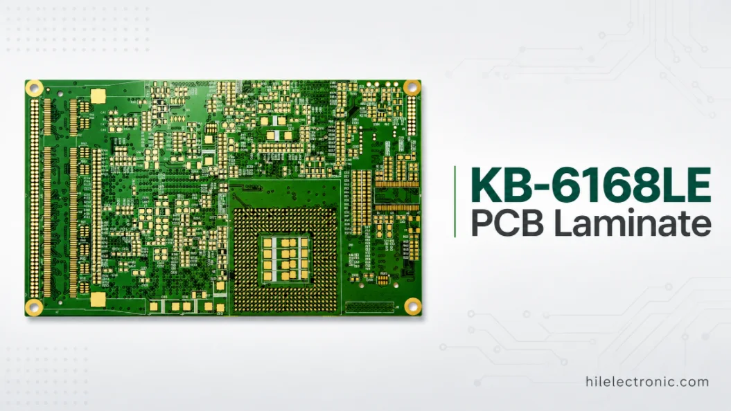
KB-6168LE PCB Laminate for Low Z-CTE Multilayer PCB Manufacturing
KB-6168LE PCB laminate is a Kingboard high-Tg, anti-CAF,...
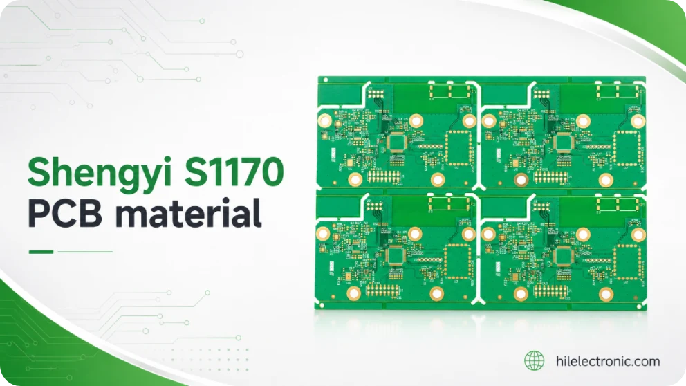
Shengyi S1170 PCB Material for High-Tg Lead-Free Multilayer PCB Manufacturing
Shengyi S1170 PCB material is a lead-free compatible,...

NP-175F PCB Laminate for High-Reliability Multilayer Boards
NP-175F PCB laminate is a Nan Ya high-Tg, filled...

High CTI FR-4 PCB Manufacturing for Insulation-Critical Boards
High CTI FR-4 is used when a PCB design needs stronger...
How to get a quote for PCBs
Let‘s run DFM/DFA analysis for you and get back to you with a report. You can upload your files securely through our website. We require the following information in order to give you a quote:
-
- Gerber, ODB++, or .pcb, spec.
- BOM list if you require assembly
- Quantity
- Turn time
In addition to PCB manufacturing, we offer a comprehensive range of electronic services, including PCB design, PCBA, and turnkey solutions. Whether you need help with prototyping, design verification, component sourcing, or mass production, we provide end-to-end support to ensure your project’s success.
For PCBA services, please provide your BOM (Bill of Materials) and any specific assembly instructions. We also offer DFM/DFA analysis to optimize your designs for manufacturability and assembly, ensuring a smooth production process.