
How to Prevent PCB Delamination for Durable Electronics

PCBs are the backbone of modern electronic devices. They serve as the platform for electrical components and connections, facilitating the proper functioning of electronic systems. However, PCBs are not immune to defects during their manufacture and assembly. One such issue that can compromise the integrity and functionality of PCBs is delamination. Delamination refers to the separation of the layers within a PCB, which can have serious consequences on the performance and reliability of the final product.
At Highleap Electronic, a leading PCB manufacturing and assembly service provider, we understand the challenges associated with PCB delamination. This guide will delve into the causes of PCB delamination, how to prevent it, and the effective methods for repairing it to ensure the durability of your electronic devices.
What Is PCB Delamination?
PCB delamination occurs when the layers of a laminated PCB start to separate or peel apart. Typically, a PCB consists of multiple layers of material bonded together under high pressure and heat. Delamination can happen when these layers lose their bond, resulting in issues such as bubbling, discoloration, or blistering on the PCB’s surface. These signs often indicate the failure of the adhesive or the material integrity, compromising the functionality of the entire circuit.
While minor delamination might be overlooked, large-scale delamination can cause performance failures, signal interference, or even complete failure of the electronic device.
Key Causes of PCB Delamination
1. Moisture Absorption
One of the leading causes of PCB delamination is moisture absorption by the PCB materials. Many PCB substrates, such as FR-4, are hygroscopic, meaning they absorb moisture from the environment. If PCBs are exposed to high humidity or improper storage conditions, moisture can penetrate the layers and weaken the bond between them. During the soldering process or thermal excursions, the trapped moisture vaporizes, leading to internal pressure and eventual layer separation.
Prevention: To prevent moisture-related delamination, PCBs must be stored in a controlled environment with low humidity. Additionally, pre-baking of PCBs before assembly helps to remove any absorbed moisture.
2. Thermal Stress and Repeated Thermal Excursions
PCBs are exposed to varying temperatures during the manufacturing process, including soldering, reflow, and wave soldering. Thermal excursions, or repeated exposure to high temperatures, can lead to delamination. If the temperature exceeds the glass transition temperature (Tg) of the PCB material, the bond between layers may weaken, causing the layers to separate. Continuous or extreme thermal cycles during the operational life of the PCB can also exacerbate delamination.
Prevention: Ensure that PCBs are fabricated using materials with a suitable Tg rating for the expected temperature conditions. High-Tg materials are essential for PCBs exposed to multiple soldering cycles or extreme temperatures.
3. Improper Soldering Techniques
Inadequate soldering profiles, such as improper reflow temperature settings or excessive heat exposure, can also lead to delamination. Reflow soldering, which involves heating the PCB to melt the solder, can result in delamination if not carefully controlled. If the PCB material is subjected to heat for too long or the temperature is too high, it can cause the layers to separate due to the thermal expansion mismatch between the layers and the base material.
Prevention: Manufacturers must adhere to strict reflow soldering profiles, ensuring optimal temperature and duration to avoid excessive heat exposure.
4. Subpar Material Quality
The quality of the raw materials used in PCB fabrication plays a critical role in preventing delamination. Poor-quality laminate materials, adhesives, or soldering materials can increase the likelihood of delamination during both the manufacturing process and during use. The use of low-quality base materials, such as improperly treated FR-4, can lead to weak bonds that are prone to separation under stress.
Prevention: Use high-quality PCB substrates and adhesives that meet industry standards. Proper selection of materials according to their application and operational environment is essential.
5. Manufacturing Defects
Delamination can also occur due to errors in the PCB fabrication process, such as improper lamination, insufficient resin application, or inadequate curing. Manufacturing defects can cause weak spots in the PCB where delamination is more likely to occur.
Prevention: Employ stringent quality control measures at every step of the PCB fabrication process. Ensure proper curing of materials and uniform resin application during lamination.
Measling vs. PCB Delamination
It’s important to distinguish between measling and delamination, as they both manifest similarly on a PCB but have different causes. Measling refers to the appearance of small, white spots on the PCB surface caused by insufficient resin application during lamination. These spots are generally small and do not affect the PCB’s functionality significantly. However, delamination, in contrast, involves the separation of the layers, often leading to more severe issues such as signal failure, short circuits, or even fire hazards.
While measling may not always affect the PCB’s performance, delamination is a serious issue that requires immediate attention.

How to Prevent PCB Delamination
1. Controlled Storage Conditions
Ensure that PCBs are stored in a dry, controlled environment. High humidity levels can lead to moisture absorption, so using sealed bags or vacuum sealing after manufacturing can help protect the PCBs from environmental moisture.
2. Pre-Baking of PCBs
Before undergoing any thermal processes, it’s crucial to pre-bake the PCBs to remove any moisture absorbed during storage. Pre-baking temperatures should exceed the boiling point of water (100°C) to ensure thorough drying.
3. Use of High-Quality Materials
Choose high-quality PCB materials with appropriate glass transition temperatures (Tg), particularly for high-performance or high-temperature applications. High-Tg materials are more resistant to thermal stress and are less likely to delaminate under extreme conditions.
4. Adherence to Soldering Profiles
Follow strict reflow soldering profiles to prevent overexposure to heat. Ensure that the soldering process uses controlled temperatures and timings, taking care to avoid overheating the PCB layers.
5. Regular Quality Control
Implement regular quality control checks during PCB fabrication, including testing for moisture content, ensuring proper curing of materials, and inspecting the uniformity of the adhesive layer. Employ techniques such as X-ray inspection to identify potential weak spots.
Repairing PCB Delamination
While the best solution is to prevent delamination during the manufacturing process, there are methods available to repair delaminated PCBs. Here’s a basic guide to repairing delamination in PCBs:
-
-
Identify the Blister or Delamination Zone: Inspect the PCB visually or through X-ray imaging to identify the delamination area. Delaminated areas often appear as raised blisters on the surface.
-
Drill Holes for Epoxy Injection: Use a micro drill to create small holes at the edges of the delaminated area. These holes allow for the injection of epoxy into the voids created by delamination.
-
Inject Epoxy: Heat the PCB to help the epoxy flow into the delaminated areas. Inject the epoxy into the drilled holes, ensuring it fills the voids thoroughly.
-
Curing: Cure the epoxy at a specified temperature (usually around 74°C or 165°F) for one hour, or at room temperature for 24 hours. After curing, scrape off any excess epoxy.
-
Testing and Inspection: Once repaired, the PCB should undergo testing to ensure that the delamination has been fully addressed and that the functionality of the PCB is restored.
-
Conclusion
PCB delamination is a critical issue that can compromise the performance and reliability of electronic devices. Understanding the causes, prevention strategies, and repair methods for delamination is essential for ensuring the long-term durability of your PCBs. By following best practices for moisture control, temperature management, and material quality, you can significantly reduce the risk of delamination.
At Highleap Electronic, we offer expert PCB manufacturing and PCB assembly services to ensure that your electronic products meet the highest standards of quality and reliability. If you’re looking for top-tier PCBs with a focus on precision and durability, reach out to us for a quote today!
Frequently Asked Questions (FAQ)
1. How can I tell if my PCB is at risk of delamination before assembly?
Before assembly, it’s crucial to inspect your PCB for signs of improper storage or handling, such as visible moisture accumulation or discoloration. To proactively detect potential delamination, you can test the PCB’s moisture content using a moisture analyzer. Additionally, conducting thermal cycle tests before assembly helps identify any vulnerabilities in the laminate material.
2. What are the common signs that PCB delamination has occurred during assembly?
Signs of delamination during PCB assembly include visible blisters or bubbles on the PCB surface, which occur when trapped moisture or thermal stress causes separation between layers. In some cases, delamination might also cause poor solder joint formation or intermittent electrical connections. These symptoms may appear during initial assembly or even after a few thermal cycles.
3. Can PCB delamination affect the performance of multilayer PCBs more than single-layer ones?
Yes, multilayer PCBs are more susceptible to the consequences of delamination. Delamination in multilayer PCBs can cause signal integrity issues, short circuits, or component misalignment, making it more critical to prevent. The more layers a PCB has, the greater the potential impact of delamination, which may lead to device failure if not addressed.
4. Is there a specific laminate material that can prevent PCB delamination?
Certain high-performance laminate materials such as high-Tg (glass transition temperature) substrates are less likely to experience delamination under extreme conditions. For applications requiring higher thermal stability or resistance to moisture, materials like Teflon (PTFE) or polyimide are also good choices. These materials help ensure a robust bond between layers even under thermal and mechanical stress.
5. What can be done to improve the long-term reliability of PCBs after delamination repair?
After repairing delamination, it’s important to subject the PCB to extended reliability testing, including thermal cycling and moisture resistance tests, to ensure the repair holds under operational conditions. Additionally, using protective coatings or encapsulation materials can help mitigate future moisture absorption and reduce the risk of further delamination.
Get a Free PCB & PCBA Quote

Recommended Posts
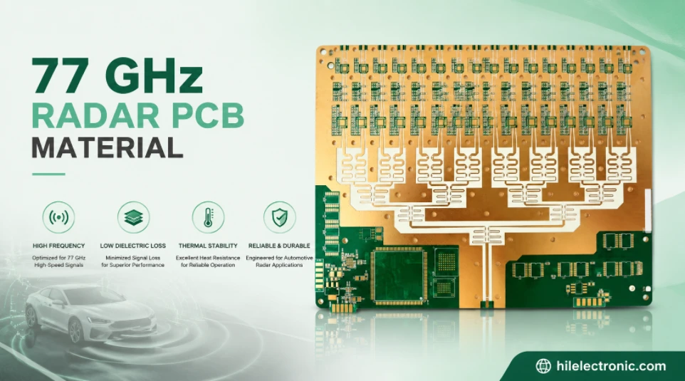
77 GHz Radar PCB Material Selection and Manufacturing Guide
Table of contentsWhat 77 GHz Changes in a PCBCommon 77 GHz...
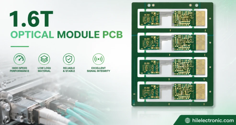
1.6T Optical Module PCB Manufacturing and Assembly Service
Table of contents1.6T Module Architectures and PCB...
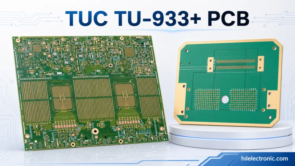
TUC TU-933+ PCB Manufacturing for Super-Low-Loss High-Speed Systems
Table of contentsWhat Is TU-933+ PCB Material?Why TU-933+...
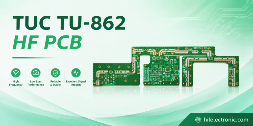
TUC TU-862 HF PCB Manufacturing and Assembly Service
Table of contentsWhat Is TU-862 HF?Why Choose TU-862 HF...
How to get a quote for PCBs
Let us run DFM/DFA analysis for you and get back to you with a report.
You can upload your files securely through our website.
We require the following information in order to give you a quote:
-
- Gerber, ODB++, or .pcb, spec.
- BOM list if you require assembly
- Quantity
- Turn time
In addition to PCB manufacturing, we offer a comprehensive range of electronic services, including PCB design, PCBA (Printed Circuit Board Assembly), and turnkey solutions. Whether you need help with prototyping, design verification, component sourcing, or mass production, we provide end-to-end support to ensure your project’s success. For PCBA services, please provide your BOM (Bill of Materials) and any specific assembly instructions. We also offer DFM/DFA analysis to optimize your designs for manufacturability and assembly, ensuring a smooth production process.