
Back to blog
Enhancing PCB Manufacturing: A Guide to Quality and Performance

Printed Circuit Boards (PCBs) are crucial components in modern electronics, serving as the backbone for various devices. With the growing demand for high-quality PCBs, it’s imperative for manufacturers to address and overcome the challenges associated with PCB production. This guide aims to provide electronics engineers, PCB designers, and manufacturing professionals with insights into common issues and practical solutions to enhance PCB quality and performance.
Plating Voids: Ensuring Robust Electrical Connections
Plating voids are tiny gaps in the copper plating of through-holes, which can compromise the board’s electrical connectivity and reliability. These voids can lead to intermittent failures, posing diagnostic challenges.
Causes:
- Contaminants in plating chemicals
- Air entrapment during the plating process
- Inadequate cleaning of drilled holes
- Insufficient copper deposition
- Poor drilling quality
Prevention Strategies:
- Implement thorough cleaning protocols post-drilling
- Optimize drilling parameters (speed, feed rate, etc.) based on material properties
- Regularly maintain and calibrate drilling equipment for precision
- Use high-quality plating solutions and monitor their composition continuously
- Employ advanced inspection methods, such as X-ray, to detect voids early in production
Copper-to-Edge Clearance
Maintaining adequate copper to edge clearance is critical for preventing environmental exposure that could lead to corrosion or shorts, ensuring long-term reliability and safety.
Best Practices:
- Follow Industry Standard Guidelines: Adhere to standard clearance guidelines, typically ranging from 0.010 to 0.015 inches.
- Consider Operating Environment: Adjust clearance margins based on the operating environment. For instance, if the Gerber file utilizes a V-CUT panelization method, a larger copper to edge clearance is necessary. Refer to the provided figure for specific data.
- Use Automatic Design Rule Checking (DRC) Tools: Employ DRC tools during the design process to ensure compliance with clearance standards.
- Conduct a Thorough Design for Manufacturability (DFM) Review: Perform a comprehensive DFM review to identify and address potential issues early in the design process.

PCB Soldering Defects
Reliable solder joints are essential for maintaining strong electrical connections and overall PCB reliability. Common issues like cold solder joints, caused by insufficient heat, and solder bridges, resulting from excess solder, can lead to functional failures and a shortened product lifespan. Additionally, problems such as insufficient solder, design errors in the Gerber file leading to solder mask leakage, and the tombstone effect, where components lift off the board, are critical to address.
To mitigate these defects, it’s important to have precise control over the soldering processes, including reflow and wave soldering, along with rigorous inspection of incoming materials. CAM engineers play a crucial role by optimizing solder mask files according to specifications, ensuring that the designs support proper solder mask bridges. Production operators must also be well-versed in the correct volume and composition of solder paste to avoid common issues.
Advanced inspection technologies, like Automatic Optical Inspection (AOI) and X-ray systems, can help identify defects early. Ensuring thorough training for manual soldering operators and strict adherence to inspection standards by QA personnel is also vital. Lastly, considering lead-free solder alternatives can help meet environmental regulations without sacrificing the quality of solder joints, ensuring a more reliable and durable product.
Slivers and Acid Traps
Splits, defined as unintended thin copper strips, and acid traps, which are sharp angles within copper traces, significantly compromise both the functionality and reliability of PCBs. These issues typically arise from design inaccuracies or inconsistencies during the etching process.
Preventing Splits:
- Adhere to Minimum Width Guidelines: Implement constraints for the minimum widths of traces and copper features to ensure structural integrity.
- Conduct Thorough DFM Checks: Utilize Design for Manufacturability (DFM) checks to proactively identify and rectify potential design flaws.
- Refine Etching Processes: Optimize the etching parameters to prevent over-etching, thus reducing the occurrence of splits.
Eliminating Acid Traps:
- Design Considerations: Design traces to avoid sharp angles less than 90 degrees, which are prone to creating acid traps.
- Utilize Advanced CAD Tools: Employ CAD software equipped with features to detect and correct acid traps.
- Adjustments in CAM Processes: When processing Gerber files, especially those with intricate designs, CAM engineers should modify the copper foil dimensions—reducing by 5 mils and increasing by 5 mils to eliminate thin copper lines. Post-adjustment, it is critical to validate the changes against the original CAD designs to ensure that vital connections, such as those involving heat sinks, are not compromised. For networks, ensure the adjustment is less than the width of the connection lines to avoid connectivity issues.
- Software Optimization: Using software like INcam for Gerber file optimization can streamline the process by setting parameters directly according to production specifications, thereby enhancing efficiency.
- Implement Automatic Smoothing: Apply design rules that automatically smooth trace crossings to further reduce the risk of acid traps.
By following these guidelines, PCB designers and manufacturers can significantly improve product quality and reduce the likelihood of failure due to splits and acid traps.
Solder Mask Defects
The solder mask protects copper traces from environmental damage and prevents solder bridges during assembly. Defects in the solder mask layer can lead to corrosion and electrical shorts.
Common Solder Mask Defects:
- Missing solder mask between pads
- Unwanted solder mask bridging
- Registration errors during application
Preventive Measures:
- Optimize solder mask thickness according to board specifications
- Ensure precise alignment and application during production
- Use high-quality solder mask materials suitable for the board’s operating conditions
- Regularly maintain application equipment to ensure consistent quality

Thermal Management: Optimizing Heat Dissipation
Thermal management in PCB design can be a bit of a tightrope walk. Getting it right is crucial because, without proper heat handling, a few common issues can crop up, potentially derailing your project. Here’s what often goes wrong:
In PCB design, thermal management issues such as component overheating, hot spots, and thermal stress can lead to decreased performance, warping, or even cracking. Additionally, prolonged exposure to heat can weaken solder joints and degrade insulation, potentially causing connection failures and electrical shorts. These complications highlight the need for effective heat control strategies to ensure PCB reliability and longevity.
Let’s explore some effective strategies to manage thermal issues effectively:
- Distribute the Heat: Utilize thermal pads and vias strategically to distribute heat more evenly across the PCB, mitigating hot spots and lowering component temperatures.
- Enhance the Copper: Thicker copper layers significantly improve heat dissipation. They function like built-in heat sinks, pulling heat away from critical components. For power PCBs requiring high current without a major design overhaul, an economical option is to solder slugs onto traces to increase their thickness.
- Intelligent Component Placement: Arrange heat-generating components thoughtfully. Space them apart and near cooling mechanisms whenever possible to enhance thermal management.
- Leverage Simulation Tools: Employ thermal simulation tools during the design phase to identify potential thermal issues early, preventing them from escalating into major problems.
- Incorporate Ventilation: Design your PCB to accommodate adequate ventilation. Often, simple airflow is sufficient to maintain optimal temperatures.
A bit of proactive planning in your PCB design can prevent extensive troubleshooting down the line. By implementing these strategies, you’re setting the stage for a cooler, more dependable PCB.

Integrating PCB Surface Finishing Techniques and Character Markings
PCB Surface Finishing Techniques
Surface finishing is a critical aspect of PCB manufacturing that enhances solderability, prevents oxidation, and ensures long-term reliability. Common surface finishes include HASL (Hot Air Solder Leveling), ENIG (Electroless Nickel Immersion Gold), and OSP (Organic Solderability Preservatives). The choice of surface finish not only depends on the PCB’s functional requirements and environmental exposures but also correlates with the trace width and spacing detailed in the Gerber files. ENIG and electroplated gold, known for their excellent surface planarity and corrosion resistance, are particularly advantageous for applications requiring minimal line width and spacing. This makes them ideal for fine-pitch components where precision is paramount.
Importance of PCB Character Markings
PCB markings, or silkscreening, provide essential information such as part numbers, component identifiers, and polarity marks, crucial for assembly and maintenance. The technology used for these markings, such as UV curing or laser etching, ensures durability and resistance to fading, thus maintaining legibility throughout the product’s lifecycle. The clarity and permanence of these markings are essential as they must endure handling and exposure to solvents without degradation.
PCB Panelization Strategies for Efficient Manufacturing
Panelization is a manufacturing technique used to optimize the assembly process by mounting multiple PCBs onto a single ‘panel’. This approach maximizes manufacturing throughput and minimizes material waste, making it particularly beneficial for high-volume production. The design of the panel must consider several factors, such as the size of the PCB, the edge clearance, and the method of separation post-assembly—usually V-scoring or tab-routing. V-scoring allows panels to be separated more easily but requires precise control to ensure that the scores do not weaken the PCBs during handling. Tab-routing offers more robust support for PCBs during assembly, especially for heavier or larger boards, but involves more complex separation post-assembly. Both methods must be carefully planned to accommodate the stress factors associated with depanelization to prevent damage to the PCBs.
In addition, effective panelization requires thoughtful layout considerations to facilitate automated assembly processes, such as pick-and-place operations, and should incorporate features like fiducial marks and tooling holes to align with manufacturing equipment accurately. Regular reviews with production teams ensure that panel designs are optimized for current manufacturing practices and equipment, reducing cycle times and enhancing overall yield. These panelization strategies, when combined with appropriate surface finishes and clear character markings, significantly contribute to the efficiency and quality of PCB manufacturing, ensuring that the boards meet stringent performance standards while remaining cost-effective.

Common EMC and EMI-Related Failures and Solutions
Electromagnetic Compatibility (EMC) and Electromagnetic Interference (EMI) are critical considerations in PCB design, especially as electronic devices become more complex and densely packed. Failures related to EMC and EMI can lead to regulatory non-compliance, signal integrity issues, and functional malfunctions. Common problems include unwanted radiation from PCBs, which can interfere with other devices, and susceptibility to external electromagnetic fields, which can disrupt the PCB’s operation.
To address these issues, here are detailed solutions:
-
Effective Grounding and Power Plane Design: Establishing a solid grounding and carefully designing power planes are essential. A well-designed ground plane reduces noise by providing a low-impedance path for return currents, minimizing the loop area, which is crucial for reducing radiated emissions. Ensure that the ground plane is continuous and avoids splits, which can create radiating structures.
-
Controlled Impedance Routing: For high-speed signals, controlled impedance routing is necessary to maintain signal integrity. This involves matching the impedance of the PCB traces to the components’ specifications, which helps prevent signal reflections and crosstalk. Differential pairs should be routed with uniform spacing and minimized length differences to maintain balance.
-
Signal Integrity Simulations: Conducting signal integrity simulations during the design phase helps identify potential sources of EMI. These simulations allow designers to visualize how signals propagate through the PCB and where interferences might occur, enabling preemptive adjustments to layout and routing.
-
Optimized PCB Stack-Up: An optimized PCB stack-up can significantly improve EMC performance. Use a stack-up that places critical signal layers adjacent to continuous ground or power planes. This configuration helps contain electromagnetic fields within the PCB, reducing emissions and susceptibility. Additionally, keeping high-speed signal layers closer to the ground plane reduces the loop area and associated noise.
-
Shielding Techniques: Where high-frequency components are used, applying shielding techniques can be effective. Shielding can be achieved through metal enclosures or dedicated ground planes. These shields help block or contain electromagnetic fields, preventing them from radiating outward or being affected by external sources. Properly connecting the shields to the ground is crucial to their effectiveness.
Designing PCBs for Harsh Environmental Conditions
Printed Circuit Boards (PCBs) are frequently deployed in environments characterized by extreme conditions, including significant fluctuations in temperature, high humidity levels, and substantial mechanical stresses. To ensure their durability and reliable performance under such demanding circumstances, it is crucial to adopt a focused design strategy tailored specifically for these challenges. This involves selecting materials that are inherently suited to withstand severe thermal and mechanical stresses, thereby maintaining structural integrity and functionality even in the harshest conditions.
Design Considerations for Harsh Environments:
- Choose materials with appropriate thermal and mechanical properties
- Apply conformal coatings to protect against moisture and contaminants
- Use strain relief methods to prevent damage from mechanical stresses
- Implement redundancy for critical systems to enhance reliability

Component Selection and Placement: Balancing Performance and Manufacturability
Selecting the right components and optimizing their placement are crucial for both the electrical performance and manufacturability of PCBs. Poor component choices can lead to issues like thermal management problems and signal integrity degradation.
Best Practices:
- Evaluate components based on availability, reliability, and environmental suitability
- Optimize placement for heat dissipation and signal integrity
- Apply Design for Assembly (DFA) principles to streamline the manufacturing process
- Use 3D modeling tools to ensure mechanical fit and avoid interference issues
Strengthening the DFM Process for Enhanced PCB Manufacturing Efficiency
A robust Design for Manufacturability (DFM) process is pivotal in preempting manufacturing complications, facilitating a reduction in production overheads and expediting market readiness. This proactive approach enables the identification and rectification of potential issues during the early stages of design, thereby optimizing the entire production cycle. Effective DFM integrates advanced automated tools that meticulously scan for prevalent design discrepancies, ensuring that all potential pitfalls are addressed prior to production commencement. This not only safeguards product integrity but also significantly mitigates the risk of costly post-production corrections.
Key Components of an Advanced DFM Strategy
The foundation of a superior DFM strategy lies in the seamless integration of several core elements. Firstly, the utilization of sophisticated automated DFM applications is essential; these tools are designed to detect and alert engineers about common and complex design anomalies that could affect manufacturability. Communication channels between the design engineers and the manufacturing floor must be open and efficient, ensuring that all design nuances are perfectly aligned with manufacturing capabilities and constraints. Customizing design rules to accommodate the specific technological and operational limits of production facilities enhances the practicality and applicability of designs. Regular collaborative reviews of design drafts, involving insights from seasoned manufacturing specialists, help in refining the designs to meet practical production demands. Moreover, maintaining an expansive repository of historical manufacturing data and established best practices serves as a valuable resource for continuous improvement and learning, thereby elevating the overall effectiveness of the DFM process.

Quality Control and Testing: Ensuring High Standards
Comprehensive quality control throughout the manufacturing process is essential to ensure the final product meets all reliability standards.
Essential Quality Control Measures:
- Implement in-line Automated Optical Inspection (AOI) at critical stages
- Use flying probe or bed-of-nails testing for thorough electrical testing
- Perform X-ray inspections for complex components like BGAs
- Conduct burn-in testing for applications requiring high reliability
- Regularly audit manufacturing processes and suppliers
Conclusion
Navigating the complexities of PCB manufacturing requires a deep understanding of common issues and the implementation of effective solutions. Addressing challenges such as plating voids, solder defects, and thermal management is crucial for improving manufacturing outcomes and enhancing product reliability.
To prevent PCB quality issues, it is essential to start with a well-thought-out design. Additionally, CAM engineers must adhere strictly to specifications and requirements. For any modified circuit board files, thorough data analysis and comparison with original CAD files are necessary to ensure consistency and avoid discrepancies or network problems. The files provided to QA engineering must be meticulously checked to confirm they align with the original design. When CAM engineers prepare the ERP process documentation, they should ensure that all critical information is included. An experienced team of CAM engineers is invaluable in addressing and mitigating common PCB problems.
Embracing advanced design and testing technologies, fostering collaboration between design and production teams, and committing to continuous improvement are key strategies for thriving in the competitive PCB industry. As the field evolves, these practices will enable professionals to meet new challenges and leverage emerging opportunities, ensuring ongoing progress in electronic design and manufacturing.

Related Articles
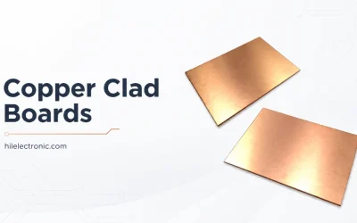
Copper Clad Boards (Copper-Clad Laminate): What They Are, Types, and How PCBs Are Made From Them
Learn what copper clad boards are, how copper clad laminate becomes a PCB, and how substrate type and copper weight affect manufacturing.

PCB QR Code Size and Placement: Design Rules for Reliable Scanning
Set PCB QR code size and placement correctly, choose a marking method, and improve scanning reliability across assembly and field service.
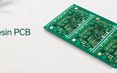
BT Resin PCB: Properties, Uses, and Fabrication Controls
Learn what a BT resin PCB is, how BT compares with FR-4, and why the laminate is used for BGA substrates and high-reliability packages.