
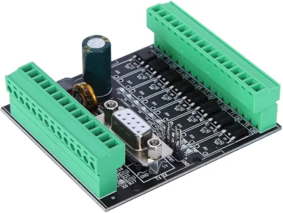
Custom PLC Board Manufacturing for Industrial Control Applications

A PLC board is not a generic industrial PCB. It is a purpose-built circuit board designed to operate continuously inside programmable logic controllers — handling processor logic, I/O signal management, power regulation, and communications in environments where electrical noise, thermal cycling, vibration, and 24/7 duty cycles are the norm rather than the exception. Getting PLC board fabrication right means making the correct decisions on materials, layer construction, copper weight, surface finish, and design rules before a single board is built.
At Highleap Electronics, we manufacture custom PLC PCBs and provide full PCB fabrication services for industrial control applications, from engineering prototype through volume production. This guide covers what separates PLC board fabrication from standard PCB manufacturing, which design decisions carry the most risk, and how to prepare a project for reliable, on-schedule production.
Table of Contents
- What Makes PLC Board Fabrication Different from Standard PCB Manufacturing
- Substrate and Material Selection for Industrial Control Environments
- Layer Stack-Up Design for PLC Boards
- EMI Control and Signal Integrity on PLC Circuit Boards
- Highleap’s PLC Board Manufacturing Capabilities
- Key Design Rules That Prevent PLC Board Failures
- Typical Applications for Custom PLC Boards
- What Files We Need for an Accurate PLC Board Quote
- PLC Board Manufacturing FAQ
What Makes PLC Board Fabrication Different from Standard PCB Manufacturing
PLC boards sit at the center of industrial automation systems. They control machinery, process sensor data, execute logic programs, and drive output devices — often without interruption for years at a time. This continuous operational requirement creates fabrication demands that standard commercial PCB manufacturing is not designed to address by default.
The key differences that define PLC board fabrication include:
- Continuous duty cycle: PLC systems run 24 hours a day, 7 days a week. Boards must be built for long-term thermal stability across thousands of power cycles, not just short-run functional testing.
- Wide operating temperature range: Industrial environments routinely require boards rated from -40°C to +85°C. Material selection, copper weight, and via design must account for repeated thermal expansion and contraction.
- Severe electrical noise environment: Variable frequency drives, servo motors, solenoids, and switching power supplies generate conducted and radiated EMI that requires careful PCB-level countermeasures to contain.
- Mixed voltage domains: PLC boards commonly carry 3.3V and 5V logic rails, 12V and 24V DC power, and in some designs 120V or 240V AC isolation sections — each requiring defined separation, clearance, and creepage distances.
- High reliability requirements: Industrial applications often demand tighter fabrication control, stronger inspection discipline, and more robust assembly quality than ordinary commercial electronics.
- Long service life expectations: Industrial equipment is expected to operate for 15 to 25 years. PLC boards must be built with materials and processes that support this service life rather than being optimized purely for initial cost.
Understanding these requirements before fabrication begins is what prevents expensive rework, field failures, and certification delays.
Upload Your PLC Board Files for DFM Review
Substrate and Material Selection for Industrial Control Environments
The base laminate material determines how a PLC board performs under thermal stress, moisture exposure, and mechanical loading across its full service life. For industrial control applications, material selection is not primarily a cost decision — it is a reliability decision.
Standard FR4 is appropriate for low-complexity PLC designs in temperature-controlled environments. For most industrial PLC applications, high-Tg FR4 (glass transition temperature 170°C or above) is the correct starting point. When a board experiences repeated thermal cycling — as is common in outdoor control panels, motor drive cabinets, and process equipment — standard FR4 laminates are more likely to suffer long-term reliability problems around vias and laminated interfaces.
| Material | Tg (°C) | Best For | Key Advantage |
|---|---|---|---|
| Standard FR4 | 130–140 | Low-complexity PLC designs in controlled environments | Cost-effective and widely supported |
| High-Tg FR4 | 170–180 | Industrial PLCs with elevated ambient temperature or thermal cycling | Better dimensional stability and reduced via barrel cracking risk |
| Halogen-free laminates | 150–175 | Safety-rated industrial and building automation PLCs | Supports halogen-free compliance requirements |
| Polyimide | 250+ | High-temperature industrial or aerospace-adjacent control applications | Exceptional thermal and chemical resistance |
| Metal-core (MCPCB) | N/A | Power supply boards and high-current output sections | Superior thermal dissipation for high-power sections |
Copper weight selection matters equally. Industrial PLC boards frequently carry supply currents of 2A to 10A or more on power planes. Specifying 1 oz copper where the design requires 2 oz is a common cause of thermal rise, voltage drop, and long-term trace degradation under sustained load.
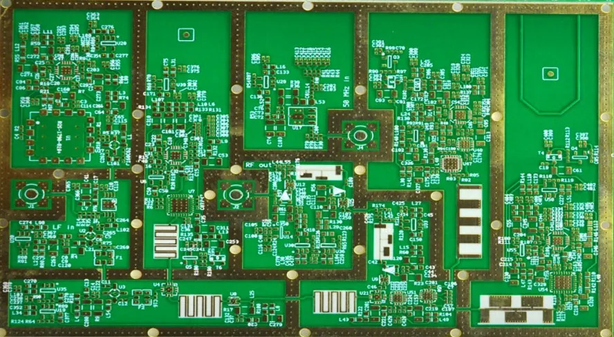
Layer Stack-Up Design for PLC Boards
PLC boards are typically built on 4 to 8 layer stack-ups. More complex designs with high-speed communication interfaces, dense I/O routing, or integrated safety functions often require 10 to 12 layers. The stack-up strategy has a direct effect on EMI performance, power distribution quality, signal integrity, and manufacturing yield.
A well-structured 4-layer PLC board stack-up uses a solid ground plane on layer 2 — often the single most important layer for EMI control — with a power plane or split power plane on layer 3. Signal routing occupies the outer layers. For 6-layer and 8-layer designs, additional layers allow separate planes for digital and analog ground domains, shielded routing of high-speed differential communication signals, and cleaner power distribution across multiple voltage rails.
The most common stack-up problems in PLC board design include:
- Split ground planes under high-frequency circuitry: Ground splits create return current discontinuities and increase radiated emissions.
- High-current traces routed adjacent to low-level analog inputs: Without adequate separation, noisy power paths can introduce measurement errors into sensitive sensor channels.
- Decoupling capacitors placed too far from supply pins: High-frequency decoupling is only effective when capacitors are placed very close to the IC power pins with direct vias to ground.
- Via stubs on high-speed signal layers in thick multilayer builds: Uncompensated via stubs can contribute to reflections and communication instability.
Early stack-up review as part of PCB design and DFM analysis helps resolve these issues before Gerber files are finalized and before fabrication cost is committed.
EMI Control and Signal Integrity on PLC Circuit Boards
EMI management is one of the most critical and most consistently underestimated aspects of PLC board design. Industrial environments are electrically hostile. Variable frequency drives generate conducted emissions across a wide frequency range. Motor contactors produce high-voltage transients. Ground loops couple noise into sensor circuits through cable shields and chassis connections.
Effective EMI control in PLC board fabrication relies on a combination of correct design practices and manufacturing precision:
- Continuous, unbroken ground planes: A solid ground plane beneath the digital circuitry section is the foundation of controlled EMI performance.
- Physical separation of high-current and low-signal areas: Power input, relay driver circuits, and high-side output stages should be physically separated from CPU, communication, and analog input sections.
- Correct decoupling strategy: Bulk capacitors close to power entry points; ceramic bypass capacitors close to each IC supply pin, with short return paths to ground.
- Controlled impedance for communication interfaces: Differential pairs for industrial Ethernet, CAN, or RS-485 require consistent trace geometry and dielectric properties to maintain target impedance. This requires impedance control PCB capability with stack-up review from your manufacturer.
- I/O port transient protection: TVS diodes at field interface connections, optical isolation on digital I/O channels, and appropriate creepage and clearance distances between isolated sections help protect both the board and external wiring.
For PLC boards that must pass EMC testing, these design elements are not optional — they are often the difference between a board that passes early and one that requires costly redesign.
Highleap’s PLC Board Manufacturing Capabilities
Building a reliable PLC board requires more than a factory that can process multilayer FR4. It requires a manufacturing partner that understands the specific requirements of industrial control electronics: reliability expectations, controlled impedance for communication layers, surface finish appropriate for connector systems, and engineering review that catches design problems before production starts.
Highleap Electronics supports PLC PCB projects from prototype through mass production, with engineering review covering stack-up feasibility, DFM compliance, surface finish selection, and assembly readiness.
| Capability | Detail |
|---|---|
| Production stage | Prototype, NPI, low-volume, and mass production |
| Layer count | 2 to 16+ layers for all PLC board types |
| Base materials | Standard FR4, high-Tg FR4, halogen-free laminates, polyimide, metal-core |
| Copper weight | 0.5 oz to 4 oz; heavier copper for high-current power sections |
| Surface finish | ENIG, HASL, ENEPIG, OSP, immersion silver — selected by connector and assembly requirements |
| Controlled impedance | Supported at ±10% and tighter tolerances for communication layers |
| Testing | 100% electrical test, AOI, impedance verification, and qualification cross-sections as required |
| Special support | Isolation slots, press-fit connector zones, selective surface treatment, edge plating, and engineering review |
For customers developing new PLC platforms, our engineering team can review stack-up proposals before Gerber files are finalized, identify potential DFM risks, and recommend material or routing adjustments that improve yield and long-term reliability.
Key Design Rules That Prevent PLC Board Failures
Most PLC board failures do not originate in the factory. They originate in the design files. A board can be electrically correct but still fail during assembly, commissioning, or long-term service if the material selection, layer construction, and design rules are not optimized for the industrial environment the board will actually operate in.
- Define reliability requirements early: Reliability, inspection level, and fabrication expectations should be locked in before release to manufacturing.
- Use thermal relief pads on high-current through-hole components: Large copper pours connected directly to power connector pins and relay terminals can create soldering problems if thermal relief is not designed correctly.
- Maintain appropriate creepage and clearance distances: PLC boards that handle multiple voltage levels must build these distances into the layout from the start.
- Design panelization for assembly: PLC boards destined for SMT assembly need tooling holes, fiducials, and panel structures that fit the downstream assembly process.
- Avoid vias under BGA packages without the right via strategy: Via-in-pad designs under processors or FPGAs may require filled and plated vias to prevent solder wicking.
- Verify solder mask expansion values: Incorrect solder mask expansion can create bridging risk at fine-pitch SMT components or pad-to-pour shorts.
These issues are far easier to resolve at the design review stage than after a production batch has been built. Every PLC board project should include early engineering review, complete fabrication notes, and well-prepared production data before release to manufacturing.
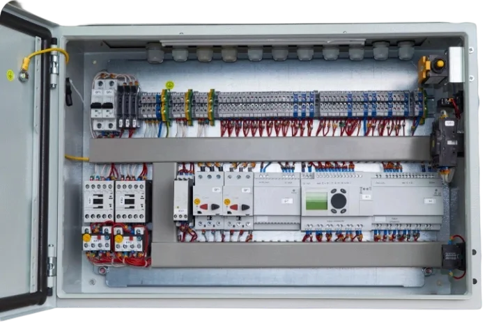
Typical Applications for Custom PLC Boards
Custom PLC board fabrication is used wherever standard off-the-shelf PLC platforms cannot meet the size, performance, cost, or supply chain requirements of the application. OEMs developing proprietary automation platforms, and end users replacing obsolete or discontinued boards, both depend on manufacturing partners who can deliver to industrial reliability expectations.
- Factory automation: machine controllers, robotic cell controllers, conveyor and sorting system PLCs, and assembly line sequencing boards
- Process control: flow, temperature, pressure, and batch process controllers for chemical, pharmaceutical, and food and beverage facilities
- Building automation: HVAC control boards, elevator and escalator controllers, fire and safety panel circuit boards
- Energy and utilities: substation automation, pump and compressor control, and renewable energy system controllers
- Transportation: traffic signal control, railway signaling, and water treatment plant automation
- Oil and gas: wellhead control panel boards and pipeline monitoring systems designed for outdoor and demanding environments
For OEM customers developing proprietary PLC platforms, we support both the programmable logic controller PCB fabrication and the downstream PCB assembly process, providing a coordinated manufacturing solution from bare board through populated and tested assembly.
What Files We Need for an Accurate PLC Board Quote
A complete and well-prepared file package reduces quoting time, prevents misunderstandings, and helps our engineering team identify potential issues before production begins. For PLC board projects, the following package provides the information needed for an accurate quote and a useful engineering review:
- Gerber files or ODB++ data: all copper layers, solder mask, silkscreen, drill files, and board outline
- Stack-up drawing: layer sequence, material specification, copper weight per layer, target board thickness, and any controlled impedance requirements
- Fabrication notes: reliability requirements, surface finish, isolation slot locations, press-fit connector zones, and any special requirements
- Mechanical drawing: board dimensions, cutout locations, connector keepout areas, and critical tolerances
- Bill of materials (if requesting assembly): full component list with manufacturer part numbers for sourcing review
- Quantity and schedule: prototype quantity, planned production volume, and required lead time
Our engineering team reviews every PLC board package for stack-up feasibility, DFM compliance, surface finish compatibility, and manufacturing risks that could delay fabrication or affect yield. This review converts a quote request into practical feedback rather than just a price.
If you are preparing a new project, you can submit your files through our PCB quote page or explore our full PCB fabrication services for production planning.
Get a Quote for Your PLC Board Project
PLC Board Manufacturing FAQ
What is the difference between a PLC board and a standard industrial PCB?
A PLC board is specifically designed for programmable logic controller applications, integrating processor, I/O management, communication, and power regulation on a board optimized for industrial environments. Standard industrial PCBs serve many functions; PLC boards are purpose-built for control applications with defined EMI, isolation, thermal, and reliability requirements.
What reliability level is appropriate for PLC board manufacturing?
Most industrial PLC applications require stricter fabrication tolerances, more thorough inspection criteria, and higher reliability expectations than ordinary commercial boards. The exact requirement depends on the end equipment, environment, and certification targets.
How many layers do PLC boards typically require?
Simple PLC designs can be built on 4-layer boards. Most mid-complexity platforms use 6 to 8 layers. High-performance PLC systems with multiple communication interfaces, dense I/O, or integrated safety functions often require 8 to 12 layers to meet EMC and signal integrity requirements.
Can you manufacture PLC boards with controlled impedance?
Yes. We support controlled impedance fabrication for PLC boards with EtherCAT, PROFINET, Ethernet/IP, CAN, or other interfaces requiring precise trace impedance. Stack-up and trace geometry are reviewed before fabrication to confirm target impedance values are achievable with the selected materials.
What surface finish is best for PLC boards?
ENIG is one of the most common choices for PLC boards. It provides a flat, solderable, and oxidation-resistant surface suitable for fine-pitch SMT components, edge connectors, and press-fit headers. For boards with predominantly through-hole assembly and no fine-pitch SMD components, HASL can be a cost-effective alternative.
Can you support both fabrication and assembly for PLC boards?
Yes. Highleap supports PCB fabrication and assembly for PLC projects, providing a coordinated manufacturing flow from bare board through fully populated and tested assembly. This reduces handoff complexity and helps maintain quality control throughout production.
What is the typical lead time for PLC board prototypes?
Lead time depends on layer count, material selection, and any special requirements such as controlled impedance or enhanced inspection. For standard multilayer builds, prototype lead times typically range from several working days to around two weeks, with rush options available for urgent development timelines.
Sabrina has over 18 years of experience in the PCB industry, with a strong background in CAM engineering and PCB file review. She supports PCB projects from prototype to volume production, focusing on manufacturability and process reliability. Her work helps engineering teams reduce production risk and achieve stable, high-quality PCB manufacturing results.

Recommended Posts
FR408HR PCB Material for High-Reliability Multilayer Boards
FR408HR PCB material is selected when a multilayer board...

Nelco N4000-13EP PCB Manufacturer for High-Reliability Multilayer Boards
Nelco N4000-13EP PCB manufacturing is used for...
Nelco N4000-13SI PCB Manufacturer for High-Speed Signal Integrity Boards
Nelco N4000-13SI PCB manufacturing is used for high-speed...
Rogers RO4450T Bondply PCB for RO4000 Multilayer RF Stackups
RO4450T bondply PCB manufacturing is a controlled...
How to get a quote for PCBs
Let us run DFM/DFA analysis for you and get back to you with a report.
You can upload your files securely through our website.
We require the following information in order to give you a quote:
-
- Gerber, ODB++, or .pcb, spec.
- BOM list if you require assembly
- Quantity
- Turn time
In addition to PCB manufacturing, we offer a comprehensive range of electronic services, including PCB design, PCBA (Printed Circuit Board Assembly), and turnkey solutions. Whether you need help with prototyping, design verification, component sourcing, or mass production, we provide end-to-end support to ensure your project’s success. For PCBA services, please provide your BOM (Bill of Materials) and any specific assembly instructions. We also offer DFM/DFA analysis to optimize your designs for manufacturability and assembly, ensuring a smooth production process.