
Back to blog
UPS PCB: The Ultimate FAQ Guide

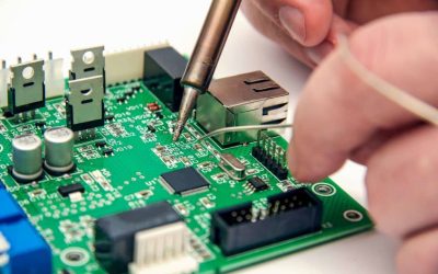
In today’s technology-driven world, uninterrupted power supply is crucial for the reliable operation of critical electronic devices and systems. Power outages and fluctuations can lead to data loss, equipment downtime, and even potential damage to sensitive components. To address these challenges, UPS PCBs have emerged as an essential component in power source management. UPS PCBs play a vital role in ensuring continuous power supply, regulating utility power, and mitigating the risks associated with unstable electrical environments.
In the upcoming sections of this guide, we will dive deeper into factors to consider when choosing a UPS PCB, discuss various types of redundant UPS PCB architectures, and compare single conversion and double conversion UPS PCB operation modes. Stay tuned for an in-depth exploration of these topics and more.
What Are The Different Types Of UPS PCB?

There are several different types of UPS (Uninterruptible Power Supply) PCB designs, each tailored to specific applications and power protection needs. Here are the common types of UPS PCB designs:
Standby UPS PCB (Offline UPS PCB)
- This type of PCB is also known as the “offline” UPS PCB and is commonly used for personal computers and small electronic devices.
- During normal operation, the standby UPS PCB allows the line voltage to charge a backup battery, which is connected to a transfer switch via an inverter.
- When a power outage occurs, the transfer switch brings the standby power online, activating the inverter to supply power from the backup battery to the load.
- The inverter is typically in standby mode and only becomes active during a power failure, hence the name “Standby UPS.”
Line Interactive UPS PCB
- Line Interactive UPS PCB is one of the most commonly used UPS designs and is suitable for a wide range of applications.
- In this design, the mains power is supplied to the inverter via a transfer switch. The inverter then supplies power to the connected load.
- The key feature of this design is the active inverter, which operates in reverse mode when the main supply is available, converting AC to DC power.
- This DC power is used to continuously charge the backup battery.
- During a blackout or power disturbance, the inverter operates in its normal direction after the transfer switch opens. It converts DC power from the battery back to AC power to supply the load.
Double Conversion Online UPS PCB
- The Double Conversion Online UPS PCB is a preferred configuration for devices with ratings beyond 10kVA and is commonly used in data centers and critical industrial applications.
- This design is similar to the standby UPS PCB but with a significant difference in the operation of the inverter.
- In the Double Conversion Online UPS PCB, the primary power path is the output of the inverter, whereas in the standby UPS PCB, it is the secondary path.
- The rectifier (AC-DC converter) is fed from the main supply and back to the inverter, which converts AC to DC power, charging the backup battery.
- The primary supply path for the load is through the inverter, which provides continuous clean power regardless of the status of the input power. This design ensures that the load is always isolated from power disturbances.
Each type of UPS PCB design has its own advantages and is suitable for specific applications. The choice of the appropriate UPS PCB design depends on factors such as the criticality of the connected equipment, load capacity, and the desired level of power protection.
Different Types Of Inverters in UPS PCB
In a UPS (Uninterruptible Power Supply) PCB, various types of inverters can be used to convert DC (Direct Current) power from the UPS’s internal battery into AC (Alternating Current) power for supplying electricity to connected devices. Each type of inverter has its own waveform and characteristics, making them suitable for different applications. The three main types of inverters commonly found in UPS PCBs are:
- Sine Wave Inverter:

- Waveform: A sine wave inverter produces an output waveform that closely resembles the smooth, sinusoidal waveform of utility grid power.
- Characteristics: Sine wave inverters provide high-quality, clean, and stable AC power. They replicate the natural form of AC power and are ideal for sensitive electronic devices and appliances.
- Suitability: Sine wave inverters are compatible with a wide range of equipment and are commonly used in applications where the quality of power supply is critical, such as homes, offices, data centers, and medical facilities.
- Modified Sine Wave Inverter:
- Waveform: A modified sine wave inverter produces an output waveform that is a stepped approximation of a sine wave, with additional steps or notches.
- Characteristics: The waveform of a modified sine wave inverter is less smooth than a pure sine wave but is still suitable for powering many electronic devices and appliances.
- Suitability: Some UPS PCBs can work well with modified sine wave inverters, although there might be a reduction in power efficiency. Modified sine wave inverters are often used in applications where cost considerations are important, but some compromise on power quality can be tolerated.
- Square Wave Inverter:
- Waveform: A square wave inverter produces an output waveform characterized by abrupt voltage transitions between two levels, typically high and low.
- Characteristics: The waveform is less smooth and more discontinuous compared to sine waves or modified sine waves, resulting in lower-quality power output.
- Suitability: Square wave inverters are the least expensive among all inverter types, but they provide the least reliable power output. They are mainly suitable for running simple devices but may not be compatible with complex UPS PCBs or sensitive electronic equipment. They are rarely used in modern applications.
The choice of inverter type in a UPS PCB depends on the specific requirements of the equipment being powered and the desired power quality. Sine wave inverters are preferred for applications where clean and stable power is essential, while modified sine wave inverters are used when a compromise between power quality and cost is acceptable. Square wave inverters are generally used in limited scenarios where the quality of power supply is not a primary concern.
UPS PCB in Power Source Management
UPS (Uninterruptible Power Supply) PCBs play a critical role in power source management, particularly in ensuring the availability of reliable backup power and optimizing the use of energy resources. Here’s how UPS PCBs are involved in power source management:
- Automatic Start-Up and Shutdown:
- UPS PCBs can control the automatic start-up and shutdown of devices connected to the UPS system. When a power outage occurs, the PCB can initiate the start-up of essential devices to maintain critical operations.
- Conversely, when power is restored or stable, the PCB can command the shutdown of non-essential equipment to conserve power and extend the runtime of the UPS system.
- Load Shedding and Prioritization:
- UPS PCBs can prioritize and shed non-essential loads during power outages to ensure that critical devices receive power for as long as possible.
- Load prioritization allows essential equipment, such as servers or medical devices, to continue operating while less critical devices are temporarily powered down.
- Scheduled Operations and Energy Conservation:
- UPS PCBs can schedule specific operations based on user-defined settings. This includes scheduling periodic system tests, battery maintenance cycles, and even powering down the entire UPS system during low-demand periods to save energy.
- Energy-saving features can help reduce electricity consumption and lower operating costs, especially in environments where backup power is rarely needed.
- Battery Management:
- UPS PCBs actively manage the UPS system’s internal battery or batteries. This includes monitoring battery health, charge levels, and temperature.
- Battery management ensures that the UPS is always ready to provide backup power when needed and prolongs the life of the battery by preventing overcharging or deep discharging.
- Remote Monitoring and Control:
- Many modern UPS systems are equipped with communication interfaces that allow remote monitoring and control of the UPS PCB’s functions.
- Through remote management, administrators can monitor the UPS’s status, receive alerts, and make adjustments to power source management settings from a centralized location.
- Energy Efficiency and Power Factor Correction:
- Some UPS PCBs incorporate power factor correction and energy-efficient features to optimize the use of power from the mains supply.
- These features improve the UPS system’s efficiency and help reduce electricity costs.
- Integration with Energy Management Systems:
- In larger installations, UPS PCBs may be integrated into broader energy management systems to coordinate power source management across the entire facility.
- Integration allows for more sophisticated load shedding, demand response, and energy conservation strategies.
In summary, UPS PCBs are central to effective power source management in environments where power reliability and energy efficiency are critical. They enable automatic control, prioritization, scheduling, and remote monitoring of power-related functions, helping organizations maintain critical operations during outages while conserving energy during stable power conditions.
Some key components commonly found on UPS PCB

A UPS PCB is a complex electronic assembly that consists of various components and circuits designed to ensure reliable and uninterrupted power supply to connected devices in the event of a power outage or voltage irregularities. Here are some of the key components typically found on a UPS PCB:
- Rectifier: The rectifier is responsible for converting incoming AC (Alternating Current) power from the utility grid into DC (Direct Current). It rectifies the AC voltage to produce a smooth DC voltage. The rectifier also charges the UPS system’s internal battery when the mains power is available.
- Inverter: The inverter is a critical component that converts DC power from the UPS’s internal battery or rectifier into AC power. It produces a stable and clean AC waveform that is used to power connected devices during a power outage. In many cases, the inverter produces a sine wave or a modified sine wave, depending on the type of UPS.
- Bypass Circuit: UPS systems often include a bypass circuit or switch that allows the input AC power to bypass the rectifier and inverter when the utility power is stable. This feature ensures energy efficiency and extends the life of the UPS components by reducing heat generation when backup power is not needed.
- Switching Devices: Various switching devices, such as relays, transistors, and thyristors, are used throughout the PCB to control the flow of power between the different components (rectifier, inverter, bypass, battery, etc.). These devices facilitate the seamless transition between utility power and battery power.
- Battery: The internal battery or battery bank is a crucial component of a UPS system. The battery stores energy when utility power is available and releases it when there is a power interruption or voltage irregularity. Battery management circuitry ensures the battery is charged and maintained properly.
- Control Logic and Microcontroller: A microcontroller or control logic circuit is responsible for monitoring the UPS system’s status, managing battery charging and discharging, controlling the inverter and bypass circuit, and making decisions regarding power source selection and transfer. It also communicates with external devices for monitoring and control purposes.
- Protection Devices: Various protection components, such as fuses, circuit breakers, and surge suppressors, are integrated into the PCB to safeguard the UPS system and connected equipment from electrical faults, overloads, and surges.
- Sensors: Sensors for monitoring temperature, humidity, and voltage levels may be incorporated into the PCB to provide data for controlling and managing the UPS system effectively.
- Communication Interface: Many modern UPS systems include a communication interface, such as RS-232, USB, Ethernet, or SNMP (Simple Network Management Protocol), allowing for remote monitoring, control, and management of the UPS through software or network connections.
These are some of the core components found on a UPS PCB. The combination of these components and the design of the PCB enable the UPS to provide reliable backup power, maintain voltage stability, and protect connected equipment from power-related issues.
Importance Of A UPS PCB
A UPS PCB plays a vital role in maintaining a stable and reliable power supply to critical electronic equipment. Its significance can be divided into three main aspects:
Preventing Data Loss and Downtime
- UPS PCBs are designed to provide backup power during interruptions in the main power supply. This function is crucial in preventing abrupt shutdowns of computers, servers, and other critical devices.
- By eliminating sudden power loss, UPS PCBs help safeguard against data corruption and loss. This is particularly vital for data centers, servers, and businesses that rely on uninterrupted data access.
Regulating Unstable Utility Power
- Utility power from the electrical grid can often be susceptible to fluctuations, voltage spikes, and surges. UPS PCBs are responsible for stabilizing and cleaning the incoming power, ensuring a consistent and reliable voltage supply.
- This regulation of power quality protects sensitive electronic equipment from potential damage caused by voltage irregularities. It also extends the lifespan of equipment and reduces the need for costly repairs or replacements.
Reducing the Risk of Component Failure and Ensuring Business Continuity
- Modern electronic components are highly sensitive to variations in power quality. Sudden power surges, spikes, or drops can lead to component failures and system malfunctions.
- UPS PCBs address this concern by providing a stable and clean power source, effectively minimizing the risk of component failure. This ensures the continuous operation of critical equipment.
- For businesses and organizations, downtime can result in significant financial losses, reduced productivity, and damage to reputation. UPS PCBs play a pivotal role in ensuring business continuity by seamlessly transitioning to backup power during power interruptions, enabling operations to continue without disruptions.
In summary, UPS PCBs are indispensable for maintaining power quality, preventing data loss, ensuring uninterrupted operation, and protecting electronic equipment from the adverse effects of power-related issues. Their importance extends to various industries and applications where a reliable power supply is critical for operational continuity and the longevity of valuable equipment.
Methods Of Mitigating EMI in UPS PCB
Mitigating Electromagnetic Interference (EMI) in UPS (Uninterruptible Power Supply) PCBs is essential for ensuring the proper functioning of the UPS system and preventing interference with other electronic equipment. Here are effective methods and techniques for reducing EMI in UPS PCB designs, divided into four parts:
1. Grounding and Ground Plane:
- Ground Plane: Implement a solid ground plane on the PCB to serve as an effective shield against EMI. A ground plane provides a low-impedance path for unwanted electromagnetic signals to dissipate, reducing the risk of interference.
- Proper Ground Connection: Ensure all ground points are properly connected to maintain a consistent ground reference throughout the PCB.
2. Layout and Trace Design:
- Trace Layout: Pay careful attention to the layout of signal traces, particularly high-speed or high-frequency traces that can emit or pick up EMI.
- Trace Length and Routing: Minimize trace lengths and keep them as short and direct as possible to reduce loop areas that can act as antennas for EMI.
- Signal Separation: Keep sensitive analog and digital signals physically separated on the PCB to prevent interference between them.
3. Component Selection and Filtering:
- EMI Filters: Incorporate EMI filters at input and output points of the UPS PCB to attenuate electromagnetic interference. These filters can reduce conducted EMI on power lines.
- Ferrite Beads and Inductors: Place ferrite beads or inductors in series with power and signal lines to suppress high-frequency noise and provide a low-impedance path for EMI currents.
- Filtering and Decoupling Capacitors: Install filtering and decoupling capacitors near sensitive components and integrated circuits to filter out high-frequency noise and stabilize power supplies.
- Proper Component Placement: Carefully select component placements to minimize the interaction between critical components and sensitive circuits.
4. Shielding and Compliance Testing:
- Shielding and Enclosures: Use shielding materials or enclosures around sensitive components or sections of the PCB to contain electromagnetic radiation.
- Sealing: Ensure that all enclosure seams are properly sealed to prevent EMI leakage.
- EMI Compliance Testing: After PCB design and assembly, conduct thorough EMI compliance testing to identify and address any residual EMI issues. Adjustments can be made based on the test results.
- Use of EMI Simulation Tools: Employ electromagnetic simulation software to analyze and optimize PCB layouts and component placement for EMI reduction.
By following these methods and techniques, UPS PCB designers can effectively mitigate EMI issues, ensuring the reliable operation of the UPS system while minimizing interference with other electronic devices.
Factors To Consider While Choosing A UPS PCB

When selecting a UPS (Uninterruptible Power Supply) PCB for a specific application, it’s essential to consider various factors to ensure that the chosen UPS PCB meets the requirements and provides reliable backup power. Here are the key factors to consider:
Topology
The first factor to consider is the topology of the UPS. You should choose the appropriate UPS topology based on your specific application’s needs. The common topologies include:
-
- Online (Double Conversion): Provides the highest level of power protection by continuously converting incoming AC power to DC and then back to AC. Ideal for critical applications with zero transfer time.
- Line-Interactive: Provides voltage regulation and battery backup while allowing the load to be powered directly from the mains when the voltage is within a specified range.
- Offline (Standby): Transfers power to the battery and inverter only when the input voltage falls outside a certain range. Suitable for less critical applications.
Rating and Capacity
The second consideration is the UPS capacity. You need to determine the required UPS capacity (in VA or watts) based on the total load that needs to be supported during power outages. Make sure that the UPS PCB can handle the load capacity effectively.
Battery Management
Battery management is critical for UPS reliability. Consider the following battery-related factors:
-
- Battery Type: Choose the appropriate battery chemistry (e.g., VRLA, lithium-ion) based on factors like expected runtime, maintenance requirements, and environmental conditions.
- Battery Autonomy: Determine how long the UPS needs to provide backup power (autonomy) and select a UPS PCB that can accommodate the required battery capacity.
- Battery Monitoring: Look for UPS PCBs with built-in battery monitoring capabilities to assess battery health and predict when replacements are needed.
Remote Monitoring and Management
The fourth factor to consider is remote monitoring and management capabilities. These features enable proactive maintenance and real-time status updates. Check if the UPS PCB supports features such as SNMP (Simple Network Management Protocol), web-based monitoring, or integration with centralized monitoring systems.
Different Types Of Redundant UPS PCB Architectures
Redundant UPS (Uninterruptible Power Supply) PCB architectures are designed to provide backup power and compensate for failures in critical applications. Each architecture offers different levels of redundancy and fault tolerance. Here are three common types of redundant UPS PCB architectures:
Zone Redundancy
-
- Zone redundancy, also known as N+X redundancy, involves dividing the critical load into multiple zones or segments, each served by its own UPS system.
- Each zone has its dedicated UPS PCB and associated battery backup.
- In the event of a failure in one zone, the other zones can continue to provide power to their respective loads without interruption.
- Zone redundancy offers a high level of fault tolerance, as failures in one zone do not affect the availability of power in other zones.
- It is suitable for applications where maintaining continuous power is critical, such as data centers and industrial facilities.
Serial Redundancy
-
- Serial redundancy, also known as N+1 redundancy, involves connecting multiple UPS systems in a serial configuration.
- One UPS system serves as the primary unit, while the others are redundant backups.
- The primary UPS PCB handles the load under normal conditions, while the redundant units remain in standby mode.
- If the primary unit fails or experiences an issue, one of the redundant units automatically takes over, providing uninterrupted power to the load.
- Serial redundancy provides a balance between fault tolerance and cost-effectiveness, as it ensures backup power while reducing the number of active UPS systems.
Parallel Redundancy
-
- Parallel redundancy, also known as 1+1 redundancy, involves running multiple UPS systems in parallel to share the load evenly.
- All UPS systems operate simultaneously, providing backup power and load-sharing capabilities.
- If one UPS system fails or encounters an issue, the remaining units continue to support the load without interruption.
- Parallel redundancy offers the highest level of fault tolerance and load-sharing capabilities but can be more complex to implement and maintain.
- It is commonly used in mission-critical applications where redundancy and load distribution are paramount.
Each type of redundant UPS PCB architecture has its advantages and considerations. The choice of architecture depends on factors such as the criticality of the application, budget constraints, and the desired level of fault tolerance. Redundant UPS systems are crucial for ensuring uninterrupted power in environments where downtime is not an option.
Single Conversion UPS PCB VS Double Conversion UPS PCB
UPS (Uninterruptible Power Supply) systems are essential for providing backup power to critical electronic equipment during power outages or disturbances. Two common types of UPS systems are single conversion (standby) UPS PCBs and double conversion (online) UPS PCBs. Let’s compare these two types based on their operation modes and efficiency:
1. Operation Modes
Single Conversion UPS PCB:
- Normal Mode: In normal operation, the UPS allows the input utility power to pass directly to the connected equipment. The inverter is in a standby mode, and the load is powered by the mains supply.
- Battery Mode: When a power outage occurs or the input voltage falls outside a specified range, the UPS switches to battery mode. It rapidly transitions to powering the load from the battery through the inverter. There is a slight transfer time during this switchover.
Double Conversion UPS PCB:
- Online Mode: In the online double conversion UPS, the input AC power is continuously converted to DC power and then back to AC power. This process is constant, ensuring that the load always receives power from the inverter, even when the utility power is stable.
- Battery Mode: During a power outage or when voltage irregularities are detected, the UPS seamlessly transitions to battery mode, but the load remains powered by the inverter. There is no transfer time, as the load is always connected to the inverter.
2. Efficiency
Single Conversion UPS PCB:
- Single conversion UPS systems tend to be less efficient compared to double conversion systems. This is because in normal operation, the UPS allows the input power to pass through without any processing, resulting in some power loss.
- Efficiency may vary based on the specific UPS model and design, but it typically ranges from 85% to 95% in normal operation.
Double Conversion UPS PCB:
- Double conversion UPS systems are known for their high efficiency, especially in online mode. Since the inverter continuously powers the load, there is no standby power loss.
- Efficiency in online mode can be as high as 95% to 98% or even higher, making double conversion UPS PCBs more energy-efficient.
3.Considerations
Single Conversion UPS PCB:
- Single conversion UPS systems are often more cost-effective and suitable for applications where occasional power outages are acceptable.
- They are commonly used for protecting non-critical equipment or in situations where the transfer time during switchover to battery mode is not a concern.
Double Conversion UPS PCB:
- Double conversion UPS systems are ideal for applications where uninterrupted power is critical, such as data centers, hospitals, and industrial processes.
- They provide the highest level of protection against power disturbances and offer superior energy efficiency.
In summary, the choice between single conversion and double conversion UPS PCBs depends on the specific needs of your application. Single conversion UPS systems are more cost-effective but may have slightly lower efficiency and a transfer time during power outages. Double conversion UPS systems offer the highest level of protection and efficiency, making them suitable for critical applications where uninterrupted power is essential.
Conclusion
Overall, proper UPS PCB specification depends chiefly on the criticality of protected equipment, depth of backup time needed, and reliability requirements, balanced against affordability constraints. Advanced remote administration and battery management capabilities found in modern boards further bolster availability and system lifespans through early issue detection. Overall, UPS circuitry plays a vital role in maintaining uninterrupted power essential for mission-critical systems.

Related Articles
What is a Cold Joint Solder and How Can You Prevent it?
By adhering to these guidelines, you can minimize the risk of cold solder joints and ensure the integrity of your PCB assemblies.
Demystifying BGA Soldering: Tips and Best Practices
Ball Grid Array (BGA) components offer many advantages, but they also come with specific challenges, particularly during the soldering process.
Selecting the Right PTFE Material for Your PCB
In this comprehensive guide, we will delve into the world of PTFE PCB technology, exploring its key properties, differences from FR4, typical applications, and more.