
High-Speed PCB Via Processing Techniques

Vias are fundamental components in multi-layer PCBs, serving as the crucial electrical connections between different layers. As the demand for faster, more reliable PCBs increases, especially in high-speed and high-frequency applications, the methods used to process vias have become more advanced and varied. The choice of via processing can have significant impacts on performance, reliability, and manufacturability. In this article, we explore the key via processing techniques used in modern high-speed PCBs and examine how they influence the overall design and performance.
Via Soldermask Opening
One of the simplest via processing techniques is leaving the via pad exposed, a method known as via soldermask opening. This technique involves creating a soldermask opening on the via pads, leaving the copper exposed. While this method is relatively straightforward, it’s typically used for specific situations such as when the vias need to be tested or measured directly. For example, when performing diagnostic checks or electrical testing, it’s essential to have direct access to the via pad.
However, this approach comes with trade-offs. Exposing the copper via pads without any protection can lead to corrosion or oxidation, particularly in high-speed designs. In applications where maintaining signal integrity is critical, such as in RF or high-frequency circuits, exposing the vias is usually not recommended. The absence of soldermask coverage increases the chances of electromagnetic interference (EMI) and signal degradation over time.

Via Covered with Soldermask
In most PCB designs, especially those requiring stable electrical performance, vias are covered with soldermask. This process involves applying soldermask over the via pad to prevent it from being exposed to external elements. The cover helps mitigate the risk of accidental shorts or unwanted connections between vias and surrounding components.
This method is commonly used in a variety of applications, from basic circuit boards to more complex designs. It’s particularly effective in ensuring electrical isolation and minimizing the possibility of signal interference. However, while the soldermask provides a protective layer, the via pad underneath remains insulated, and the copper is sealed off from direct contact with external surfaces.
It’s important to be mindful of the via diameter when using this method—typically, vias with a diameter larger than 0.5mm can present challenges in ensuring a clean and effective soldermask application. Larger vias may require additional steps to ensure that the soldermask opening is perfectly aligned and that no unwanted gaps remain in the design.

Via Filled with Soldermask
In some cases, the via isn’t just covered with soldermask, but completely filled with the material. The via filled with soldermask method is designed to offer a more robust solution, particularly when the PCB requires additional stability and mechanical integrity. By completely filling the via with soldermask, you essentially seal it off, preventing any solder from flowing into the via during the soldering process. This ensures the via remains fully insulated and avoids the potential for solder wicking into the hole.
The benefits of this approach are evident in multi-layer PCBs and high-density designs, where vias need to be reliably sealed to prevent unwanted connections. In these applications, the filled vias provide a cleaner assembly process and can help with thermal management, although there are limitations regarding the maximum size of the vias that can be effectively filled. For vias larger than 0.5mm, ensuring complete fill can become increasingly challenging, and voids or gaps may remain, which can lead to reliability issues.

Via Filled with Resin
For more complex and high-reliability designs, particularly when dealing with blind vias (those that don’t go all the way through the PCB), a resin fill is often necessary. This technique uses an epoxy resin to fill the via, providing mechanical stability and preventing delamination during the PCB lamination process. Resin-filled vias also ensure better soldering quality, especially when vias are drilled on solder pads, where failure to properly fill the via could lead to poor solder joints and compromised electrical connections.
While resin-filled vias enhance the mechanical robustness of the PCB, they also add a layer of protection against material flow during lamination. However, this method does introduce a thermal challenge. Resin, while effective for structural stability, doesn’t provide the thermal conductivity needed for high-power applications, and it may increase thermal resistance in certain designs. This is particularly critical in high-power applications, such as those found in automotive electronics, where managing heat effectively is essential.

Via Filled with Copper Paste
The via filled with copper paste method is particularly valuable in applications where both thermal management and signal integrity are paramount. Here, the via is filled with copper paste after the via walls have been plated. The copper paste improves the via’s thermal conductivity, making it ideal for high-power systems such as 5G circuits, automotive electronics, and high-frequency communication systems.
Copper-filled vias are designed to handle high currents and heat dissipation. The thermal conductivity of copper paste is significantly higher than resin or soldermask, making it a superior choice when managing high temperatures is critical. This process is also beneficial for high-speed signal integrity because the added copper helps reduce impedance and signal reflection, which can otherwise degrade performance in sensitive applications.
One of the challenges with copper paste filling is ensuring uniformity in the fill process. Overfilling or undercutting the via can result in unreliable connections or improper heat dissipation. Additionally, the via’s surface must be carefully leveled during manufacturing to avoid voids or defects that could compromise both the mechanical integrity and thermal performance.

Differences Between the Five Via Hole Processing Methods
Via Covered with Soldermask vs. Via Filled with Soldermask
The main difference between these two methods lies in the extent of solder mask coverage. Via covered with soldermask involves applying soldermask over the pad of the via, leaving the rest of the via exposed. This provides basic coverage, ensuring the pad is protected from contaminants and reducing the risk of short circuits. On the other hand, via filled with soldermask involves completely filling the via with soldermask, effectively sealing the entire hole. This creates a non-translucent appearance and can prevent solder from flowing into the via during assembly, improving the PCB’s durability and functionality.
Via Covered with Soldermask vs. Soldermask Opening
Via covered with soldermask refers to the soldermask application that fully covers the solder pad of the via, protecting it from external elements. In contrast, soldermask opening leaves the solder pad of the via exposed by not covering it with soldermask. This exposed area allows for further surface treatments, such as tin plating, which can make the via pad suitable for surface-mount soldering or interconnections. While soldermask opening facilitates easier assembly in certain cases, it increases the risk of contamination or short circuits if not carefully controlled.
Via Covered with Soldermask Opening vs. Via Filled with Soldermask
Via covered with soldermask opening leaves the via pad exposed, allowing light to pass through the hole, which can be useful for visual inspections or other testing purposes. However, this method does not fully seal the via. Via filled with soldermask, by contrast, involves filling the entire via with soldermask, effectively sealing the hole and making the via non-translucent. This method is often preferred in designs where preventing contamination or protecting the via from solder wicking is critical.
Via Filled with Resin vs. Via Filled with Copper Paste
The primary difference between via filled with resin and via filled with copper paste lies in the materials used and their intended applications. Via filled with resin uses epoxy resin to fill the via, which is commonly done in blind vias to prevent delamination during lamination. This method is effective for maintaining structural integrity but does not contribute significantly to heat dissipation. In contrast, via filled with copper paste uses high-thermal conductivity copper paste to fill the via, which is essential for high-performance PCBs that require better heat management. Copper paste has a high thermal conductivity coefficient (8 W/m·K), making it ideal for high-power or high-frequency applications where thermal control is a concern.
Comparison of Via Processing Methods

Engineers usually confirm this topic together with Rogers laminate PCB fabrication and AlN and alumina PCB when preparing a reliable PCB or PCBA build.
Conclusion
In high-speed and high-frequency PCB design, the processing of vias plays a critical role in ensuring optimal performance. Each via treatment method offers distinct benefits and considerations, and choosing the right method depends on the specific demands of the application. Whether the focus is on electrical isolation, mechanical robustness, signal integrity, or thermal management, understanding the strengths and limitations of each via processing technique is key.
For engineers working with high-speed PCBs, it’s essential to carefully assess the project requirements before deciding on a via treatment method. For example, high-power applications may benefit from copper paste-filled vias, while multi-layer, high-density designs might prioritize via filled with soldermask for ease of assembly. In any case, choosing the right via method is crucial to ensuring the long-term reliability and performance of the finished PCB.
At Highleap Electronic, we specialize in producing high-performance PCBs tailored to meet the specific needs of each project. With our expertise in advanced via processing and PCB assembly, we ensure that every aspect of your design is optimized for both performance and manufacturability. Reach out to us today to discuss how we can help bring your next high-speed PCB project to life.
FAQs
1. What is the purpose of using via soldermask opening in PCB design?
Via soldermask opening is typically used when direct access to the via is needed for testing or measurement purposes. However, it comes with risks like solder bridging or solder wicking near SMT pads, which could lead to short circuits during assembly. This method is best used in prototype designs where testing is crucial.
2. How does via covered with soldermask enhance PCB reliability?
Via covered with soldermask prevents exposed vias from causing short circuits or electromagnetic interference (EMI) by ensuring the via’s pad is fully covered. However, if the via diameter exceeds 0.5mm, achieving proper soldermask coverage can become challenging, leading to potential coverage gaps.
3. What are the challenges with via filled with soldermask?
Via filled with soldermask seals the via to prevent solder from flowing into it, improving mechanical strength and long-term durability. However, filling larger vias (over 0.5mm) can be difficult, as incomplete filling may occur, potentially compromising performance or structural integrity.
4. When should you use via filled with resin in PCB manufacturing?
Via filled with resin is commonly used in blind vias to prevent delamination during lamination and improve the overall solderability. While it’s effective for maintaining structural integrity, resin has lower thermal conductivity than other materials, which may cause issues in high-power applications.
5. What are the advantages of using via filled with copper paste?
Via filled with copper paste enhances thermal conductivity and signal integrity, making it ideal for high-frequency or high-power applications. However, it’s a more complex and expensive process, requiring precise application to avoid issues like thermal hotspots or poor conductivity, adding to the overall cost and manufacturing time.
Get a Free PCB & PCBA Quote

Recommended Posts
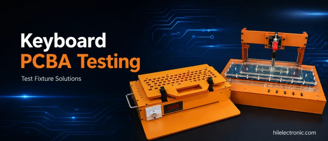
Keyboard PCBA Testing & Firmware Programming
Table of contentsKeyboard PCB Functional Testing Scope and...

Hall Effect Keyboard PCB Manufacturing & PCBA
Table of contentsHall Effect Keyboard PCB Buying...

ZMK Keyboard PCB Manufacturing & Assembly
Table of contentsZMK Wireless Keyboard PCBA Procurement...

Wireless Mechanical Keyboard PCB Manufacturing
Table of contentsWireless Keyboard PCB Procurement...
How to get a quote for PCBs
Let us run DFM/DFA analysis for you and get back to you with a report.
You can upload your files securely through our website.
We require the following information in order to give you a quote:
-
- Gerber, ODB++, or .pcb, spec.
- BOM list if you require assembly
- Quantity
- Turn time
In addition to PCB manufacturing, we offer a comprehensive range of electronic services, including PCB design, PCBA (Printed Circuit Board Assembly), and turnkey solutions. Whether you need help with prototyping, design verification, component sourcing, or mass production, we provide end-to-end support to ensure your project’s success. For PCBA services, please provide your BOM (Bill of Materials) and any specific assembly instructions. We also offer DFM/DFA analysis to optimize your designs for manufacturability and assembly, ensuring a smooth production process.