
Huawei Flash Transfer vs. Bluetooth

In today’s fast-evolving technology landscape, innovations that improve data transfer and device communication are crucial to industries like PCB manufacturing and assembly. Huawei’s Flash Transfer technology is one such breakthrough that can indirectly influence the hardware design of PCBs, offering new possibilities for device connectivity and performance. By understanding how Huawei’s Flash Transfer works and its implications on PCB design, manufacturers can adapt their processes to stay ahead in a highly competitive market.
What is Huawei’s Flash Transfer Technology?
Huawei’s Flash Transfer is a high-speed wireless data transfer solution that allows devices to rapidly exchange large amounts of data. The core of this technology is its ability to establish ultra-fast connections between devices, typically smartphones, tablets, or PCs, without relying on traditional methods such as Wi-Fi or Bluetooth. Flash Transfer achieves this through a combination of advanced communication protocols and proprietary algorithms that significantly enhance transfer speeds, latency, and overall performance.
The technology operates by leveraging a combination of near-field communication (NFC), high-speed wireless protocols, and optimized data transmission methods. It enables users to transfer large files, images, videos, or other data quickly between devices without the need for a physical connection. This innovation is poised to revolutionize the way we think about wireless communication, with a significant impact on industries relying on high-performance electronics, such as PCB manufacturing.
The Impact of Flash Transfer Technology on PCB Design and Development
While Huawei’s Flash Transfer is primarily a software solution, its effects on hardware, particularly PCB design and manufacturing, cannot be understated. To support Flash Transfer’s high-speed, low-latency communication, the underlying hardware—specifically the PCB—needs to accommodate the specific requirements of the technology. Let’s explore some of the ways in which Flash Transfer can influence PCB design and development.
1. Increased Demand for High-Speed Data Transfer Capabilities in PCBs
For Flash Transfer to function at its full potential, the devices involved must have PCBs that support high-speed data transfer. This means that PCB designs need to incorporate more advanced technologies, such as:
-
- High-Speed Signal Routing: To achieve fast, reliable communication between components, PCBs need precise and well-optimized signal routing to minimize noise and interference.
- Impedance Control: Ensuring that the impedance of high-speed signal traces on the PCB is well-controlled is critical for maintaining signal integrity.
- Advanced Materials: High-speed data transfer often requires the use of materials with lower signal loss and better performance at higher frequencies. Advanced laminates and materials like PTFE (Polytetrafluoroethylene) and high-frequency ceramics might be used in PCB manufacturing to support Flash Transfer.
These changes in design and material selection contribute to the overall performance of devices utilizing Huawei’s Flash Transfer, which directly impacts the PCB manufacturing process.
2. Miniaturization and Compact Design
Huawei’s Flash Transfer technology is designed for devices with increasingly compact form factors, such as smartphones, wearables, and other IoT devices. As devices become smaller, PCB designs must also evolve. PCB manufacturers will face the challenge of integrating complex wireless communication capabilities into smaller and more compact boards.
Miniaturized PCB designs require:
-
- Microvia Technology: This allows for denser designs and more complex circuit layouts that are required for high-speed, low-latency data transfer.
- Stacked Components: To save space, components may be stacked or mounted on both sides of the PCB, making the manufacturing process more intricate.
Adapting to these miniaturization trends while ensuring high-speed communication will be crucial for PCB manufacturers working with devices featuring Huawei’s Flash Transfer technology.
3. Power Efficiency in PCB Design
As Flash Transfer technology facilitates faster data transfers, it also demands more power. For devices like smartphones, tablets, and wearables to run efficiently without draining battery life, PCB designs need to optimize power delivery and consumption. Advanced power management techniques such as voltage regulators, low-power components, and optimized power distribution networks are essential.
Flash Transfer devices will likely feature low-power chipsets, and efficient power distribution will be a critical consideration for PCB designers. This means designing PCBs with:
-
- Low-Power Circuitry: Components that consume minimal power while still enabling high-speed transfers.
- Thermal Management: Effective heat dissipation methods to ensure that devices don’t overheat during high-data transfers, potentially requiring advanced heat sink integration into PCB layouts.
4. Reliability and Durability of PCB Designs
With Huawei’s Flash Transfer technology aiming for rapid, constant data exchanges, the reliability of the PCB is of utmost importance. As devices engage in more frequent data transfers, they experience increased wear and tear, which could impact the PCB’s long-term durability. To ensure optimal performance, PCB manufacturers need to focus on:
-
- Durable Soldering Techniques: To withstand continuous data exchanges and high-frequency signals.
- Robust Connections: Ensuring that the PCB’s connections to wireless modules and antennas are strong enough to maintain a reliable data link over time.
Designers will also need to consider the impact of environmental factors, such as heat, moisture, and electromagnetic interference, on the performance of Flash Transfer devices.

The Role of PCB Manufacturers in Supporting Flash Transfer
For PCB manufacturers, adapting to the needs of Flash Transfer technology requires a deep understanding of the requirements for high-speed data transfer. Manufacturers must ensure that their PCBs can support the specific needs of devices that rely on this technology. This means:
Adopting Advanced PCB Design Techniques: Manufacturers must stay ahead of trends in high-frequency circuit design, such as implementing controlled impedance, signal integrity optimization, and power management strategies.
Upgrading Manufacturing Capabilities: The increasing complexity of PCBs for Flash Transfer devices may require more advanced fabrication processes. High-density interconnect (HDI) technology and multi-layer boards will likely be necessary for miniaturized designs.
Ensuring Compatibility: For devices featuring Flash Transfer, PCB manufacturers need to ensure that they can integrate the necessary wireless communication modules (like NFC or proprietary Huawei modules) while maintaining compatibility with the entire device ecosystem.
Flash Transfer vs. Bluetooth
One of the key differences between Huawei’s Flash Transfer and Bluetooth technology lies in their performance and use cases, which can have significant implications for PCB design and manufacturing. Let’s explore how the two compare:
1. Data Transfer Speed
-
- Flash Transfer: Flash Transfer is designed to offer much higher data transfer speeds compared to traditional wireless protocols. While Bluetooth can support speeds of up to 3 Mbps (in Bluetooth 2.0), Flash Transfer can achieve data transfer rates of up to 1 Gbps, which is up to 300 times faster. This makes Flash Transfer ideal for transferring large files, like high-definition videos or high-resolution images, without delay.
- Bluetooth: Bluetooth, especially in its low-energy form (Bluetooth LE), is optimized for low power consumption and is suitable for transmitting smaller amounts of data over longer periods. However, it is not designed to handle the volume or speed of data transfers that Flash Transfer can manage.
2. Latency
-
- Flash Transfer: Flash Transfer offers ultra-low latency, meaning there is minimal delay when transferring data between devices. This is particularly beneficial in use cases requiring real-time synchronization or rapid communication, such as in multimedia sharing or device control.
- Bluetooth: Bluetooth typically has higher latency than Flash Transfer. Although it is acceptable for everyday uses like wireless audio streaming, its latency is less suited for real-time applications requiring immediate data exchange.
3. Power Efficiency
-
- Flash Transfer: While Flash Transfer provides high-speed data transfer, it does consume more power than Bluetooth. This is due to its need for faster data rates and optimized communication protocols. However, this can be mitigated by integrating efficient power management into the device’s PCB design.
- Bluetooth: One of the key advantages of Bluetooth, particularly Bluetooth LE (Low Energy), is its power efficiency. Bluetooth devices can operate for extended periods on a small battery, which makes it ideal for applications such as wearables, wireless peripherals, and IoT devices.
4. Range
-
- Flash Transfer: Flash Transfer typically operates over shorter distances, often within a few meters, which makes it ideal for direct device-to-device communication, like transferring files between two smartphones or laptops.
- Bluetooth: Bluetooth, depending on the version and class, can offer a longer range, up to 100 meters (with Bluetooth 5.0), making it more suitable for applications where devices need to communicate over greater distances, such as in smart home systems or wireless speakers.
5. Use Cases
-
- Flash Transfer: Flash Transfer is most beneficial in scenarios where speed and data volume are paramount. This includes high-performance applications like transferring large media files, software updates, or even large datasets for industrial IoT devices.
- Bluetooth: Bluetooth is ideal for applications with low data transfer requirements, such as wireless audio, remote control devices, or wearable sensors, where speed is not as critical but power efficiency and range are more important.
Conclusion
Huawei’s Flash Transfer technology is a major leap forward in wireless data transfer, and its implementation in consumer devices will drive changes in how PCBs are designed and manufactured. PCB manufacturers must adapt to these changes by optimizing their designs for high-speed communication, miniaturization, power efficiency, and reliability. As devices that rely on this technology become more widespread, the demand for advanced PCBs will grow, offering a unique opportunity for forward-thinking PCB manufacturers to innovate and stay competitive.
FAQs
1. What is the purpose of using via soldermask opening in PCB design?
Via soldermask opening is typically used when direct access to the via is needed for testing or measurement purposes. However, it comes with risks like solder bridging or solder wicking near SMT pads, which could lead to short circuits during assembly. This method is best used in prototype designs where testing is crucial.
2. How does via covered with soldermask enhance PCB reliability?
Via covered with soldermask prevents exposed vias from causing short circuits or electromagnetic interference (EMI) by ensuring the via’s pad is fully covered. However, if the via diameter exceeds 0.5mm, achieving proper soldermask coverage can become challenging, leading to potential coverage gaps.
3. What are the challenges with via filled with soldermask?
Via filled with soldermask seals the via to prevent solder from flowing into it, improving mechanical strength and long-term durability. However, filling larger vias (over 0.5mm) can be difficult, as incomplete filling may occur, potentially compromising performance or structural integrity.
4. When should you use via filled with resin in PCB manufacturing?
Via filled with resin is commonly used in blind vias to prevent delamination during lamination and improve the overall solderability. While it’s effective for maintaining structural integrity, resin has lower thermal conductivity than other materials, which may cause issues in high-power applications.
5. What are the advantages of using via filled with copper paste?
Via filled with copper paste enhances thermal conductivity and signal integrity, making it ideal for high-frequency or high-power applications. However, it’s a more complex and expensive process, requiring precise application to avoid issues like thermal hotspots or poor conductivity, adding to the overall cost and manufacturing time.
Get a Free PCB & PCBA Quote

Recommended Posts
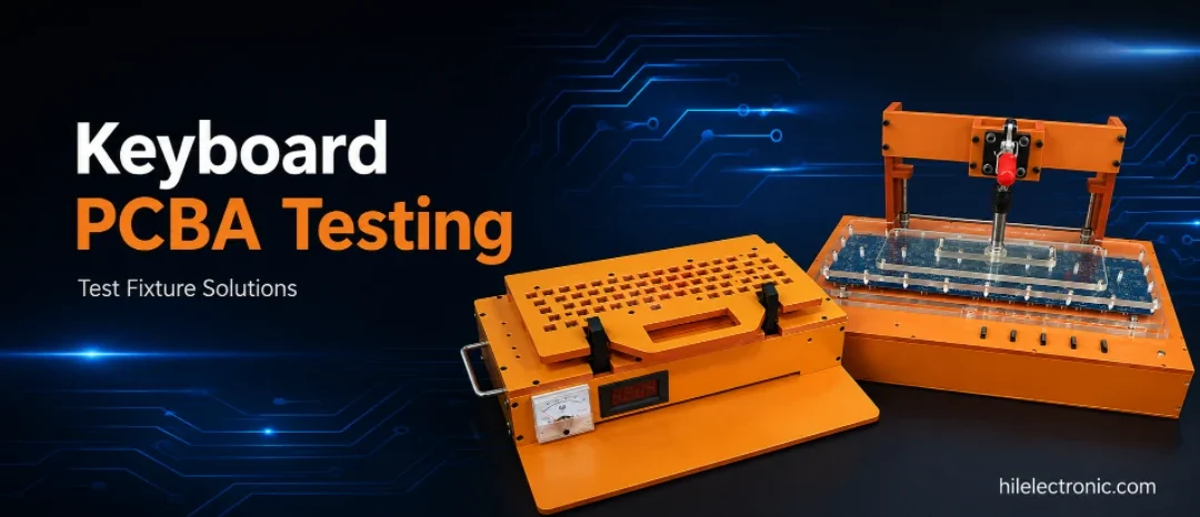
Keyboard PCBA Testing & Firmware Programming
Table of contentsKeyboard PCB Functional Testing Scope and...

Hall Effect Keyboard PCB Manufacturing & PCBA
Table of contentsHall Effect Keyboard PCB Buying...

ZMK Keyboard PCB Manufacturing & Assembly
Table of contentsZMK Wireless Keyboard PCBA Procurement...

Wireless Mechanical Keyboard PCB Manufacturing
Table of contentsWireless Keyboard PCB Procurement...
How to get a quote for PCBs
Let us run DFM/DFA analysis for you and get back to you with a report.
You can upload your files securely through our website.
We require the following information in order to give you a quote:
-
- Gerber, ODB++, or .pcb, spec.
- BOM list if you require assembly
- Quantity
- Turn time
In addition to PCB manufacturing, we offer a comprehensive range of electronic services, including PCB design, PCBA (Printed Circuit Board Assembly), and turnkey solutions. Whether you need help with prototyping, design verification, component sourcing, or mass production, we provide end-to-end support to ensure your project’s success. For PCBA services, please provide your BOM (Bill of Materials) and any specific assembly instructions. We also offer DFM/DFA analysis to optimize your designs for manufacturability and assembly, ensuring a smooth production process.