
When to Use Bare PCB

Bare PCBs refer to circuit boards that do not yet have any components mounted on them. Essentially, a bare PCB is a foundation of electronic devices made up of substrate material, typically fiberglass-reinforced epoxy resin (FR4), and conductive copper layers that form the circuits and traces. These boards play a critical role in electronics, as they provide the platform where all components, such as resistors, capacitors, microcontrollers, and other active or passive devices, will be soldered.
Although bare PCBs seem simple in appearance, their applications are vast and diverse. Understanding when to use bare PCBs can be crucial for manufacturers, hobbyists, and engineers working on a variety of electronic projects. This article delves deep into the key scenarios where bare PCBs are appropriate, along with the benefits and limitations of using them. Additionally, we’ll explore the critical aspects that determine the selection of bare boards for various applications.
1. What is a Bare PCB?
A Bare PCB is essentially the blank canvas of an electronic circuit. It includes layers of substrate material (usually FR4) and conductive pathways made of copper that connect different points on the board. These pathways, or traces, are etched onto the copper layers in patterns that form the electronic circuit. The bare PCB also includes drilled holes for vias and component mounting. There are no electrical components soldered onto it yet; it is only the physical structure of the circuit board without any functionality until components are assembled.
Key elements of a bare PCB include:
- Copper Traces: Pathways that carry electrical signals between components.
- Pads: Exposed areas of copper where components will be soldered.
- Vias: Plated through-holes that connect different layers of the PCB.
- Substrate: The insulating material (e.g., FR4) that provides mechanical support.
Bare PCBs come in various types, such as single-sided, double-sided, and multilayer boards, depending on the complexity of the circuits.
2. When to Use Bare PCBs?
There are several specific scenarios where using bare PCBs is advantageous. These applications span from the early stages of product development to large-scale manufacturing. Let’s examine the most common situations when bare PCBs are used:
2.1 Prototyping and Development
One of the most common uses of bare PCBs is in the prototyping and development phase of electronic products. Engineers and designers use bare boards to create prototype circuits before committing to mass production. During the prototyping stage, bare PCBs allow developers to test the electrical characteristics, functionality, and layout of the circuit. Bare PCBs provide a cost-effective way to experiment with design changes and optimize the circuit layout before proceeding to the final production stage.
Advantages of using bare PCBs for prototyping:
- Cost-Effective: Bare PCBs are relatively inexpensive, especially for single-sided or double-sided designs, allowing multiple iterations of the prototype without significant expense.
- Flexibility in Design: Engineers can easily make adjustments to the circuit layout or design, ensuring that any potential issues can be identified and resolved early in the development process.
- Verification: Bare PCBs allow for complete electrical and mechanical testing of the circuit before components are mounted.
Bare PCBs in prototyping are essential for identifying issues with trace routing, power delivery, or component placement that may not be evident until physical testing occurs. Once a design is validated on a bare PCB, it can then proceed to mass production.
2.2 Low-Cost Consumer Electronics
Bare PCBs are extensively used in the production of low-cost consumer electronics. Many electronic devices, such as calculators, remote controls, or basic home appliances, use simple circuits that can be easily accommodated on single or double-sided bare PCBs. These products require mass production at a low cost, and bare boards provide a cost-effective solution without compromising performance.
In such cases, the simplicity of the circuitry often doesn’t necessitate multilayer boards or sophisticated component mounting techniques. Bare PCBs are assembled with basic through-hole or surface-mounted components and are often designed for easy and rapid assembly.
Advantages in low-cost consumer electronics:
- Economical Manufacturing: Bare PCBs are a low-cost solution for mass production, making them suitable for budget-friendly consumer products.
- Efficient Assembly: Simple designs allow for fast and automated assembly processes, further reducing production costs.
- Adequate for Basic Circuits: The bare PCB is sufficient to handle the functionality required in low-power, low-complexity devices.
2.3 Custom Circuit Design for Specific Applications
For engineers, designers, and hobbyists working on custom circuit designs for specific projects or applications, bare PCBs are often the best choice. Custom bare boards can be tailored to meet unique electrical and mechanical requirements. These projects may involve designing specific circuitry for niche applications, such as robotics, home automation systems, or custom industrial controls.
Bare PCBs offer customization flexibility:
- Custom Layouts: Designers can develop specific layouts suited to their project needs, optimizing trace routing and component placement for efficiency or specific performance criteria.
- Small Batch Production: Bare PCBs allow small batch production runs for niche projects or custom electronics that may not require large-scale manufacturing.
- High Precision: For applications requiring specific routing, controlled impedance, or thermal management, custom bare PCBs provide the necessary foundation for optimal circuit performance.
Hobbyists also benefit from using bare PCBs in DIY electronics projects, as they provide a professional look and reliable performance compared to breadboards or perf boards.
2.4 Simplified Circuits for Educational Purposes
In educational settings, bare PCBs are commonly used for teaching electronics, circuit design, and soldering techniques. Educational institutions often use bare boards for students to learn how to assemble, troubleshoot, and test basic circuits.
Using bare PCBs in educational environments helps students:
- Understand Circuit Design: By working with bare boards, students gain a hands-on understanding of how circuits are constructed, how signals flow, and how to troubleshoot issues.
- Practice Soldering: Bare PCBs provide the perfect platform for learning how to solder components onto a board, a critical skill in electronics.
- Develop Problem-Solving Skills: Working with bare PCBs helps students learn how to identify and solve issues with electrical circuits, preparing them for real-world engineering challenges.
Bare PCBs used in educational kits often come with simple circuit layouts and pre-drilled holes to make assembly straightforward and conducive to learning.
3. Advantages of Using Bare PCBs
Bare PCBs offer several significant advantages that make them a preferred choice in various applications. First and foremost, cost efficiency stands out as a primary benefit. Since bare boards are produced without any components, they are significantly less expensive than fully assembled PCBs, making them ideal for prototyping, educational use, and large-scale production where minimizing costs is essential. Additionally, customization flexibility is another major advantage; designers have complete control over the layout of traces, vias, and pad sizes, enabling tailored solutions for specialized projects that may not be achievable with standard PCBs.
Furthermore, bare PCBs facilitate ease of testing and troubleshooting, allowing comprehensive electrical evaluations before components are mounted. This early detection of potential issues—such as trace routing problems or grounding inefficiencies—can save valuable time and resources. Lastly, they provide a fast turnaround time in rapid prototyping scenarios. Designers can obtain bare boards within days, enabling immediate testing and iteration of their designs. This speed is particularly beneficial in fast-paced environments where timely market entry is crucial, ensuring that projects remain on schedule and within budget.
If you’re looking for a comprehensive solution for PCB manufacturing and assembly, contact us today. Our expert team is ready to provide tailored services that meet your specific needs and ensure your project’s success from start to finish.

4. Limitations of Bare PCBs
Despite their benefits, bare PCBs come with several limitations that must be considered:
4.1 Lack of Functionality
Bare PCBs, by definition, lack any electronic functionality until components are assembled onto the board. Therefore, they serve only as a structural platform and cannot be tested for full functionality until after the assembly process is complete.
4.2 Limited Use in Complex Designs
While bare PCBs work well for simple circuits, they are not always suitable for more complex designs. In multilayer PCBs or circuits requiring precise impedance control, more advanced techniques are needed during the design and manufacturing process. As circuit complexity increases, the limitations of a bare board may require additional layers or more sophisticated design techniques, driving up costs.
4.3 Assembly Costs and Expertise Required
Although bare PCBs are inexpensive to produce, assembling them requires specialized skills and equipment, such as soldering irons or pick-and-place machines. If a project does not have access to the necessary expertise or tools, the overall cost can increase significantly.
Conclusion
Bare PCBs are fundamental building blocks in the electronics industry, providing essential platforms for circuit designs across various applications. Understanding when to use bare PCBs can help engineers, manufacturers, and hobbyists make informed decisions in product development, prototyping, and assembly processes. From simple educational projects to complex industrial applications, bare PCBs offer flexibility, cost efficiency, and ease of customization that are invaluable in the electronics realm.
At Highleap Electronic, we offer end-to-end PCB and PCBA manufacturing solutions, providing high-quality bare PCBs as well as complete PCB assembly (PCBA) services. Whether you need customized bare boards for prototyping or fully assembled PCBs for large-scale production, our advanced manufacturing capabilities and experienced team guarantee reliability, precision, and cost-efficiency. Let us take your project from design to production seamlessly—contact us today to see how we can bring your electronics innovation to life!
Get a Free PCB & PCBA Quote

Recommended Posts
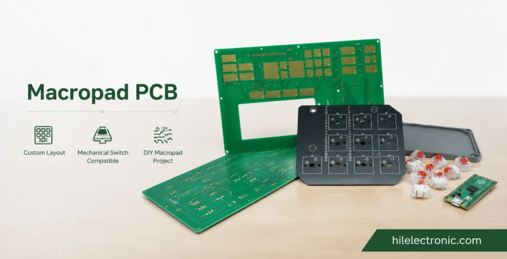
Macropad PCB Manufacturing & Custom PCBA
Table of contentsMacropad PCB Buying Guide and Quick...
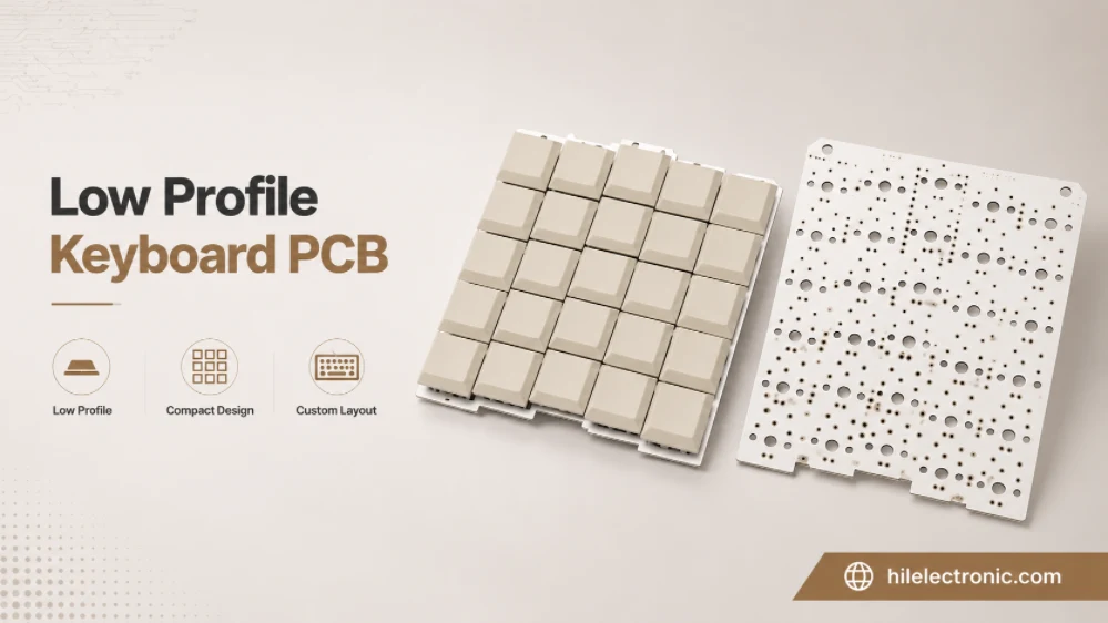
Low-Profile Keyboard PCB Manufacturing & Assembly
Table of contentsLow Profile and Choc Keyboard PCBA...
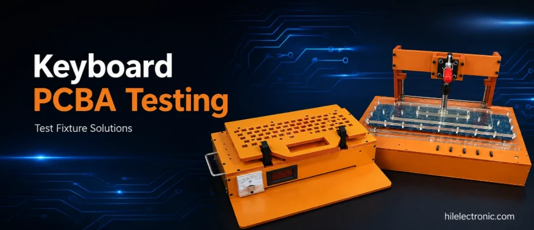
Keyboard PCBA Testing & Firmware Programming
Table of contentsKeyboard PCB Functional Testing Scope and...

Hall Effect Keyboard PCB Manufacturing & PCBA
Table of contentsHall Effect Keyboard PCB Buying...
How to get a quote for PCBs
Let us run DFM/DFA analysis for you and get back to you with a report.
You can upload your files securely through our website.
We require the following information in order to give you a quote:
-
- Gerber, ODB++, or .pcb, spec.
- BOM list if you require assembly
- Quantity
- Turn time
In addition to PCB manufacturing, we offer a comprehensive range of electronic services, including PCB design, PCBA (Printed Circuit Board Assembly), and turnkey solutions. Whether you need help with prototyping, design verification, component sourcing, or mass production, we provide end-to-end support to ensure your project’s success. For PCBA services, please provide your BOM (Bill of Materials) and any specific assembly instructions. We also offer DFM/DFA analysis to optimize your designs for manufacturability and assembly, ensuring a smooth production process.