
Thermal Conductivity Coefficient of Copper in PCBs

Copper is one of the most critical materials in the design and manufacturing of printed circuit boards (PCBs), primarily because of its excellent thermal and electrical properties. One of the defining characteristics of copper is its high thermal conductivity, which plays a crucial role in the performance, reliability, and longevity of PCBs, especially in high-power and high-temperature applications.
The thermal conductivity coefficient of copper, which is approximately 400 W/m·K at room temperature, makes it an ideal material for dissipating heat from electronic components. This guide will explore how the thermal conductivity coefficient of copper impacts PCB design, manufacturing, and application, while also diving into its benefits, challenges, and solutions for optimizing PCB performance in thermal management.
Thermal Conductivity and Its Importance in PCBs
Thermal conductivity is a material’s ability to conduct heat. It’s a key property that determines how efficiently heat can flow through a material when subjected to a temperature gradient. For PCBs, effective heat dissipation is critical to avoid overheating, which can degrade performance, damage components, or even cause complete system failure.
Copper’s high thermal conductivity means it can efficiently transfer heat away from components that generate a lot of thermal energy, such as power transistors, LEDs, CPUs, and other heat-sensitive devices. As heat generation in electronic devices continues to increase due to growing power densities and shrinking form factors, the role of copper in managing thermal performance has become even more vital.
Key Concepts:
- Thermal Conductivity Coefficient (k): This refers to the amount of heat that can be transferred through a material. For copper, this value is 400 W/m·K.
- Heat Dissipation: Effective removal of heat from electronic components, primarily facilitated by copper in PCBs.
- Thermal Management: The strategies employed in PCB design to minimize heat buildup and optimize cooling.
Role of Copper in PCB Thermal Management
Copper is primarily used in the form of traces, vias, and planes within PCBs, acting both as electrical pathways and as thermal conduits. The layout of copper traces and planes plays a significant role in managing heat within the PCB, distributing it away from heat sources to cooler areas or external heat sinks.
Copper Layers in PCBs
A typical PCB consists of multiple layers, with copper being used extensively in the inner and outer layers. The copper thickness and the way it is arranged directly affect the board’s ability to dissipate heat. Thicker copper layers can handle higher current loads and also improve thermal conductivity, allowing the PCB to manage more heat.
- Standard Copper Thickness: The typical thickness of copper in PCBs ranges from 1 oz/ft² (35 µm thick) to 2 oz/ft² (70 µm thick). However, high-current and high-heat applications may require heavy copper PCBs, which can have copper thicknesses of 3 oz/ft² (105 µm) or more.
- Heavy Copper PCBs: These are often used in high-power applications where thermal management is critical. The increased copper thickness provides a greater surface area for heat dissipation, allowing the board to handle higher temperatures and power loads without damaging the components.
Copper Planes and Traces
Copper planes, especially ground and power planes, serve as large surfaces that can distribute heat efficiently across the PCB. Copper traces, which connect various components, can also be designed with wider widths or greater thickness to improve their heat-handling capability. Wider traces reduce the thermal resistance of the copper, allowing heat to flow more freely.
- Power and Ground Planes: These planes act as heat spreaders, distributing thermal energy across the PCB surface and reducing hot spots.
- Wider Traces for Heat Dissipation: Traces that carry high currents should be wide enough to minimize electrical resistance and maximize heat dissipation.
Vias for Thermal Management
Thermal vias are another important aspect of copper’s role in PCB heat dissipation. These vias, which are essentially copper-plated holes that connect different layers of the PCB, allow heat to pass from the surface layer into the inner copper layers or even to the opposite side of the board. This technique is especially useful in multi-layer PCBs, where copper layers can be stacked to enhance heat spreading.
- Thermal Vias: Used to connect copper layers and transfer heat vertically through the PCB.
- Via Density: Increasing the number of thermal vias in heat-sensitive areas can significantly improve heat dissipation.
Challenges of Copper-Based Thermal Management
While copper’s high thermal conductivity offers many advantages in PCB design, there are also several challenges that designers must navigate.
Balancing Electrical and Thermal Design
Copper serves both electrical and thermal purposes in a PCB, so there can be a trade-off between optimizing the PCB for electrical performance and for thermal management. Increasing the width of copper traces for better heat dissipation may affect signal integrity, particularly in high-speed circuits where impedance control is critical.
Managing Copper Costs
Copper is relatively expensive compared to other materials used in PCBs, and increasing copper thickness or the number of copper layers in a board can raise manufacturing costs. Heavy copper PCBs, in particular, are more costly to produce, and the additional material requirements may impact the overall budget of the project.
Thermal Expansion and Mechanical Stress
Copper’s thermal expansion coefficient, though relatively low compared to other metals, still needs to be considered in PCB design. The mismatch in the thermal expansion rates of copper and the substrate material (typically FR-4) can cause mechanical stress during temperature cycling, which may lead to warping, cracking, or delamination over time.
- Thermal Expansion Mismatch: The difference in expansion rates between copper and the PCB substrate material can cause stress during thermal cycling.
- Mechanical Reliability: Ensuring the mechanical reliability of the PCB over time requires careful consideration of how copper layers expand and contract with temperature changes.

Optimizing PCB Design for Thermal Management Using Copper
To maximize the benefits of copper’s high thermal conductivity in PCB design, several strategies can be employed. These include using thicker copper layers, designing wider traces, and incorporating thermal vias and heat sinks. Here are some key design considerations:
Increasing Copper Thickness
As mentioned earlier, thicker copper layers allow for better heat dissipation. In high-power applications, it’s common to use heavy copper PCBs to improve thermal management. Increasing copper thickness not only enhances heat dissipation but also allows the board to carry higher currents without overheating.
- Heavy Copper PCBs: Suitable for applications like power supplies, motor controllers, and LED lighting, where large amounts of heat are generated.
- Design Trade-offs: While thicker copper layers improve thermal performance, they may require adjustments to the PCB design to accommodate the increased layer thickness, which can affect the overall board dimensions.
Utilizing Thermal Vias
Thermal vias play an essential role in distributing heat across multiple PCB layers. By connecting copper planes on different layers, these vias provide a pathway for heat to escape from the surface of the board. Designers can optimize the number and placement of thermal vias to improve the board’s overall heat-handling capabilities.
- Optimizing Via Placement: Placing thermal vias near heat-generating components can help distribute heat more effectively across the PCB.
- Filled Vias: In some cases, vias can be filled with conductive materials to further enhance heat transfer.
Integrating Heat Sinks and Copper Heat Spreaders
In some designs, copper heat spreaders or external heat sinks are used to manage thermal loads. These components can be attached to the PCB surface, allowing heat to dissipate more efficiently into the surrounding environment.
- Heat Spreaders: Large copper areas designed specifically for thermal dissipation, often connected to the PCB’s copper layers through thermal vias.
- External Heat Sinks: Additional heat sinks made from materials with high thermal conductivity (like aluminum or copper) can be attached to the PCB to draw heat away from critical components.
Component Placement and Board Layout
Strategic component placement and PCB layout can also play a role in thermal management. Heat-generating components should be placed in areas where heat can be dissipated efficiently, such as near copper planes or thermal vias. Additionally, keeping high-power components away from sensitive areas helps prevent heat from affecting critical parts of the circuit.
- Component Clustering: Avoid clustering high-power components together, as this can create localized hot spots.
- Airflow Considerations: Ensure that the PCB layout allows for proper airflow around heat-generating components to facilitate natural or forced convection.
Application-Specific Thermal Management Solutions Using Copper
Power Electronics: In power electronics, PCBs must handle significant heat due to high current flows. Heavy copper PCBs, with copper layers as thick as 10 oz/ft², are used in these applications to manage both the electrical load and associated heat. These heavy copper layers function as both conductors and thermal pathways, preventing overheating. This technology is critical in high-power devices like industrial power supplies, motor controllers, and converters, where thermal reliability is a key concern.
LED PCBs: LEDs produce substantial heat that must be managed effectively to ensure consistent performance and longevity. Metal-core PCBs (MCPCBs), which incorporate a thick copper layer combined with a metal core, are frequently used in LED applications. This design helps distribute heat away from the LEDs more efficiently than traditional PCBs, preventing thermal degradation. MCPCBs are especially vital in high-power LED lighting, where heat dissipation is crucial to maintaining light output and device durability.
Automotive Electronics: Automotive systems, especially those in the powertrain, require PCBs that can withstand extreme temperature fluctuations and high currents. Copper plays a critical role in thermal management in these applications, where thermally optimized copper layers ensure that heat generated during operation is effectively dissipated. This helps prevent overheating in components such as engine control units and power distribution modules, which are essential for vehicle reliability and safety.
High-Frequency Applications: In high-frequency PCBs, such as those used in RF and microwave circuits, thermal management is essential to maintain signal integrity. Copper’s high thermal conductivity allows it to dissipate heat efficiently, which is crucial for preventing signal degradation caused by excessive heat. This is particularly important in high-power transmission systems, where maintaining stable temperatures ensures optimal performance and long-term reliability.
Conclusion
The thermal conductivity coefficient of copper plays a crucial role in the design and performance of PCBs, particularly in applications that generate substantial heat. Copper’s high thermal conductivity allows it to dissipate heat efficiently, helping to prevent component failure and ensuring the longevity of the board.
By understanding how copper layers, traces, vias, and heat sinks contribute to thermal management, PCB designers can optimize their layouts for both electrical and thermal performance. Despite some challenges—such as balancing cost, electrical performance, and mechanical stress—copper remains the material of choice for thermal management in PCBs.
As technology continues to evolve, the importance of copper in managing heat in increasingly powerful and compact devices will only grow. Through thoughtful design and careful consideration of copper’s thermal properties, engineers can continue to push the boundaries of PCB performance while maintaining reliable thermal management.
Get a Free PCB & PCBA Quote

Recommended Posts
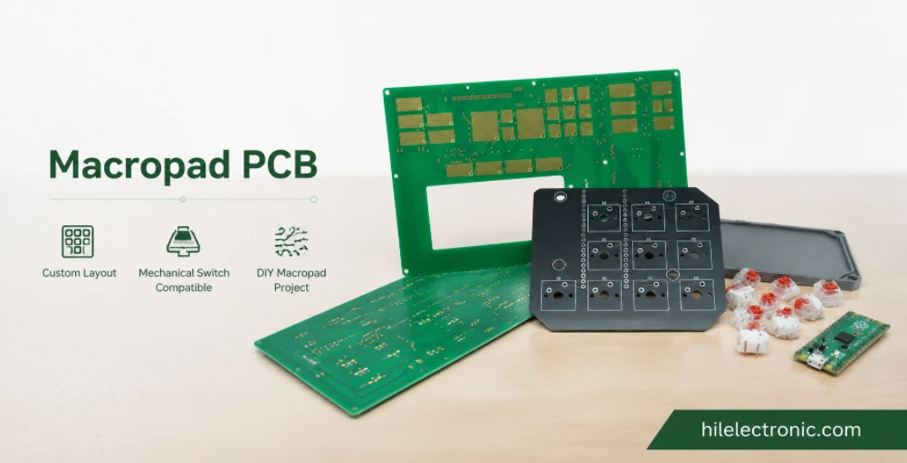
Macropad PCB Manufacturing & Custom PCBA
Table of contentsMacropad PCB Buying Guide and Quick...
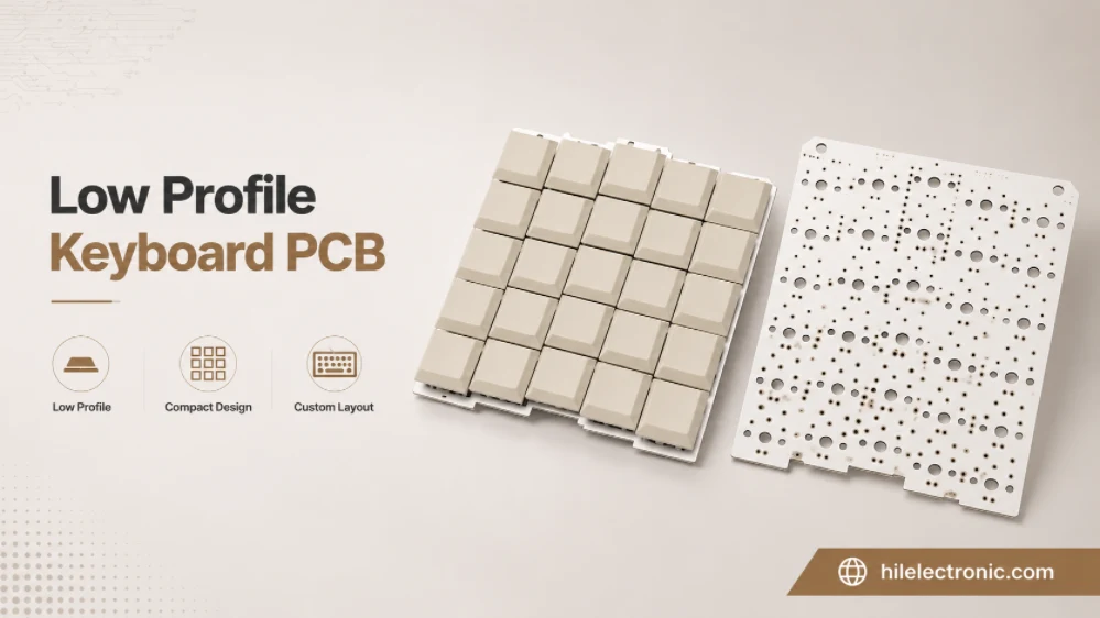
Low-Profile Keyboard PCB Manufacturing & Assembly
Table of contentsLow Profile and Choc Keyboard PCBA...

Keyboard PCBA Testing & Firmware Programming
Table of contentsKeyboard PCB Functional Testing Scope and...

Hall Effect Keyboard PCB Manufacturing & PCBA
Table of contentsHall Effect Keyboard PCB Buying...
How to get a quote for PCBs
Let us run DFM/DFA analysis for you and get back to you with a report.
You can upload your files securely through our website.
We require the following information in order to give you a quote:
-
- Gerber, ODB++, or .pcb, spec.
- BOM list if you require assembly
- Quantity
- Turn time
In addition to PCB manufacturing, we offer a comprehensive range of electronic services, including PCB design, PCBA (Printed Circuit Board Assembly), and turnkey solutions. Whether you need help with prototyping, design verification, component sourcing, or mass production, we provide end-to-end support to ensure your project’s success. For PCBA services, please provide your BOM (Bill of Materials) and any specific assembly instructions. We also offer DFM/DFA analysis to optimize your designs for manufacturability and assembly, ensuring a smooth production process.