
The Impact of PCB Design Features on Production PCB Expenses

The cost of manufacturing PCBs can vary widely based on several factors, including the board’s design, materials, and complexity. Understanding PCB expenses is crucial for optimizing production and reducing overall costs without compromising performance. Discover how hole size, number of holes, trace width, and PCB thickness affect production costs. Learn to navigate manufacturing complexities and optimize designs to reduce costs.
1. Material Selection: The Foundation of PCB Expenses
The type of material used in a PCB plays a significant role in its cost. PCBs can be made from a variety of materials, each offering different characteristics suited for specific applications.
1.1 FR4 and Standard Materials
For most standard applications, FR4 is the go-to material due to its balance of affordability, durability, and electrical performance. FR4 is a glass-reinforced epoxy laminate that offers good insulation and thermal properties, making it suitable for a wide range of electronic devices, from household gadgets to computers.
1.2 High-Performance Materials
However, not all PCBs can use FR4. High-performance PCBs, such as those used in aerospace or medical devices, often require advanced materials that can withstand extreme conditions. These materials include Rogers laminates, polyimide, and PTFE, which offer superior thermal reliability, chemical resistance, and signal integrity.
- Thermal Reliability: High-performance PCBs must handle extreme temperatures without warping or losing functionality. Materials like polyimide offer higher thermal reliability compared to standard FR4.
- Signal Integrity: For high-frequency applications like microwave and RF circuits, materials with better dielectric properties are required to ensure the accuracy and speed of signal transmission. Rogers materials, for example, are often used in such cases.
Using these specialized materials can significantly increase costs—sometimes as much as 10 times more expensive than standard FR4 boards. This increase is due to both the cost of the materials themselves and the specialized processes required for manufacturing and testing.
2. PCB Size
The size of a PCB is another crucial factor that affects its price. Larger boards require more material, take longer to manufacture, and involve more intricate assembly processes, all of which contribute to higher expenses.
2.1 Panel Utilization
PCBs are typically produced in panels, which are sheets of material where multiple boards are laid out before being separated. Efficient panel utilization is critical to minimizing waste and reducing costs. The better a board design fits into the panel’s layout, the more cost-effective it will be.
For example, an 18×24 inch PCB panel that is fully utilized with minimal gaps between boards will be less expensive to produce than one where significant material is wasted due to inefficient spacing or design.
2.2 Design Complexity and Component Density
PCB design also impacts the cost, particularly when it comes to component density. A smaller board that packs numerous components into a limited space can actually be more expensive to produce than a larger, simpler board. High-density PCBs often require more intricate routing and smaller trace widths, which increase the complexity and time needed for manufacturing.
Ultimately, the balance between board size and component density must be optimized to ensure that the PCB is both cost-effective and meets performance requirements.
3. PCB Layers
PCBs can consist of multiple layers, with each additional layer increasing the complexity of manufacturing. While a simple PCB may only have one or two layers, more advanced designs, such as those found in smartphones, laptops, or industrial equipment, often feature multiple layers to accommodate more complex circuits.
3.1 Cost Breakdown by Layer Count
As the number of layers increases, so does the cost of production. Here’s a general breakdown of how costs rise with additional layers:
- 1 Layer to 2 Layers: A cost increase of 35% to 40%.
- 2 Layers to 4 Layers: An additional 35% to 40%.
- 4 Layers to 6 Layers: A further 30% to 40%.
- 6 Layers to 8 Layers: Another 30% to 35%.
- 8 Layers to 10 Layers: An increase of 20% to 30%.
- 10 Layers to 12 Layers: A final increase of 20% to 30%.
This rising cost is primarily due to the additional materials required, the need for precise alignment between layers, and the increased risk of manufacturing defects as the board becomes more complex. Multilayer PCBs require additional lamination and drilling processes, which also add time to the production cycle.
3.2 Signal Integrity and Layer Count
In some cases, more layers are necessary to maintain signal integrity, especially for high-speed or high-frequency circuits. Multiple layers can help to separate power and ground planes from signal traces, reducing interference and ensuring reliable operation.

4. PCB Surface Finish
The type of surface finish used on a PCB also affects its cost. The surface finish protects the exposed copper traces and pads from oxidation, ensuring long-term reliability and solderability.
4.1 Common PCB Surface Finishes
Here are some common surface finishes, each with its own cost and performance implications:
- HASL (Hot Air Solder Leveling): One of the most common and cost-effective finishes, HASL provides good solderability but may not be ideal for more delicate components.
- ENIG (Electroless Nickel Immersion Gold): A more expensive option, ENIG offers better durability, corrosion resistance, and reliability, making it suitable for high-performance and long-life applications.
- OSP (Organic Solderability Preservative): Another low-cost option, OSP provides good solderability but has a limited shelf life compared to other finishes.
The choice of surface finish should be based on the intended application and environmental conditions the PCB will face. More advanced finishes, like ENIG, can increase costs slightly but offer improved performance in demanding environments.
4.2 Less Common PCB Surface Finishes: Advantages and Disadvantages
While common PCB surface finishes like HASL, ENIG, and OSP are widely used, there are several less common finishes that may offer specialized benefits for certain applications. Each of these alternatives has its own set of advantages and disadvantages that can significantly impact the overall performance and cost of a PCB.
Immersion Silver (ImAg):Immersion silver is known for its excellent solderability and flat surface, making it suitable for high-frequency applications. This finish provides a cost-effective alternative to ENIG while still offering good corrosion resistance. However, one of its significant drawbacks is its susceptibility to tarnishing, which can affect performance over time, especially if the boards are stored in unfavorable conditions. Additionally, immersion silver has a relatively short shelf life, making it less ideal for applications that require long-term storage.
Immersion Tin (ImSn):Immersion tin is another viable option, particularly in lead-free PCB designs. It offers excellent solderability and a flat surface, making it suitable for surface-mount technology (SMT). While it is relatively cost-effective, immersion tin also has its downsides, such as a limited shelf life and the risk of tin whisker formation, which can lead to short circuits. These factors make it essential for designers to weigh the pros and cons when considering this finish for their projects.
Hard Gold (Electrolytic Gold):Hard gold is primarily used for connectors and edge fingers due to its exceptional durability and high conductivity. This finish provides excellent electrical performance and wear resistance, making it ideal for components that undergo frequent mechanical interactions. However, hard gold is significantly more expensive than other finishes, which can limit its use to specific areas of the PCB rather than as a blanket finish. The higher costs associated with hard gold plating require careful consideration of budget and application needs.
ENEPIG:ENEPIG is a versatile finish compatible with various wire-bonding technologies. It offers excellent corrosion resistance and high-quality solder joints, making it suitable for advanced applications that demand reliability. However, ENEPIG is one of the most expensive surface finishes available due to its complex deposition process and the use of precious metals like palladium and gold. The complexity of this process can also lead to increased lead times, making it a consideration for projects with tight schedules.
5. Hole Sizes, Minimum Trace Width and Spacing, PCB Thickness and Aspect Ratio
The size and number of holes in a PCB can have a substantial impact on production costs. More holes require additional labor and materials, particularly if they are small and need specialized tools for precise drilling. Complex designs with numerous small holes increase both the time and cost involved in manufacturing. Additionally, thicker boards add to this complexity, as they are harder to drill, further driving up expenses due to the difficulty of working with stronger materials and increased layer thickness.
Trace width, which refers to the conductive pathways on a PCB, plays a critical role in ensuring the board’s electrical efficiency. Wider traces are necessary for higher current-carrying capacity, but they also come with added costs due to more intricate design and layout considerations. Proper planning of trace width and spacing is essential to avoid overheating and maintain reliability. Extra costs may also arise from applying additional solder masks to protect traces from electrical surges, which adds another layer of complexity to the design process.
PCB thickness and aspect ratio are also key factors that affect costs. The standard PCB thickness is typically around 1.6 mm, but advanced applications may require thicker boards. As thickness increases, so do the production costs, due to the need for more materials and the challenges involved in manufacturing. Boards with multiple layers or a larger aspect ratio are particularly expensive because they involve more work and materials to produce, making them significantly more costly to manufacture.
6. Custom Specifications
Custom designs in PCB manufacturing can lead to increased expenses due to their unique specifications and requirements. For example, elements like contoured edges or side-plating for enhanced electromagnetic compatibility not only require specialized tools but also demand skilled labor, which adds to production time and costs. Moreover, custom features may involve additional processing steps, such as increasing the thickness of gold fingers by 2 microns for improved conductivity or opting for full board plating with hard gold to enhance durability and performance. These intricate specifications necessitate careful planning and communication with manufacturers to ensure all requirements are met without unexpected cost increases.
The complexity of custom production processes significantly impacts overall expenses. Incorporating features like unique solder mask clearances or specialized drill patterns can require specific machinery and techniques that are not standard in typical PCB production. This not only raises labor costs but may also lead to longer lead times, further increasing costs. Understanding these implications beforehand is crucial for budget management and helps in anticipating potential delays or additional charges associated with custom requests.
In addition to specialized features, the choice of materials can also influence the final price. For instance, opting for higher-grade substrates or specialized finishes, such as electroless nickel immersion gold (ENIG) or other premium surface treatments, can enhance performance but will inevitably increase the manufacturing costs. Therefore, it is essential to weigh the benefits of custom specifications against their financial impact to achieve a balance between performance and cost-effectiveness in PCB design.
Conclusion
Understanding PCB expenses involves various factors, including material selection, size, layer count, finishes, hole specifications, trace requirements, thickness, panelization, solder mask options, and silkscreen colors. Each of these elements significantly impacts production costs.
By analyzing these factors, designers can make informed decisions that balance performance and budget. Early collaboration with PCB manufacturers clarifies specifications and costs, ensuring the final product meets both functional and financial requirements.
Investing wisely in materials and design can lead to substantial savings, especially in high-volume applications. As the electronics industry evolves, staying updated on advancements is crucial for optimal results.
At Highleap Electronic, we offer high-quality PCB and PCBA solutions tailored to your needs. If you’re looking to optimize your PCB expenses, please contact us today!
Get a Free PCB & PCBA Quote

Recommended Posts
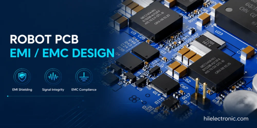
Robot PCB EMI/EMC Design for Reliable Robotics
Robot PCB EMI and EMC design affects whether a robot can...
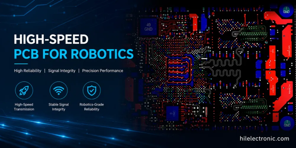
High-Speed PCB for Robotics: PCIe, DDR, MIPI and Ethernet Layout
High-speed PCB manufacturing for robotics supports data...
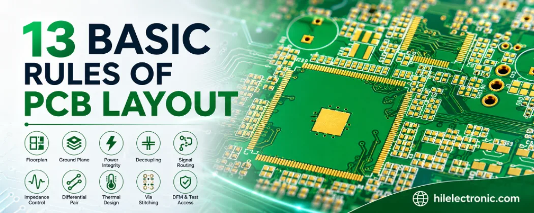
13 Basic Rules of PCB Layout (and the Failures They Prevent)
Figure 1. 13 Basic Rules Of Pcb Layout reference image for...

PCB Current Calculator: Sizing Trace Width and Vias with the IPC-2221 Formula
Figure 1. Pcb Current Calculator reference image for PCB...
How to get a quote for PCBs
Let us run DFM/DFA analysis for you and get back to you with a report.
You can upload your files securely through our website.
We require the following information in order to give you a quote:
-
- Gerber, ODB++, or .pcb, spec.
- BOM list if you require assembly
- Quantity
- Turn time
In addition to PCB manufacturing, we offer a comprehensive range of electronic services, including PCB design, PCBA (Printed Circuit Board Assembly), and turnkey solutions. Whether you need help with prototyping, design verification, component sourcing, or mass production, we provide end-to-end support to ensure your project’s success. For PCBA services, please provide your BOM (Bill of Materials) and any specific assembly instructions. We also offer DFM/DFA analysis to optimize your designs for manufacturability and assembly, ensuring a smooth production process.