
Reliable PCB Manufacturing and Assembly Services for Wireless Charging Technologies

In today’s fast-paced world, wireless charging has revolutionized how we power our devices, offering unparalleled convenience and efficiency. Also known as wireless power transfer (WPT) or inductive charging, this technology eliminates the clutter of cables, providing a seamless user experience. For businesses looking to manufacture Wireless Charging PCBs and wireless charging products, partnering with a reliable PCB manufacturer is crucial. Highleap Electronic, a leader in PCB manufacturing and assembly, is your ideal partner in bringing cutting-edge wireless charging solutions to market.
Understanding Wireless Charging
Wireless charging encompasses a variety of terms that are often used interchangeably, each highlighting different aspects of the technology:
-
- Wireless Power Transfer (WPT): A broad term covering all methods of transmitting electrical energy without wires.
- Inductive Charging: A specific method of WPT that uses electromagnetic fields to transfer energy between coils.
- Qi Charging: A widely adopted standard developed by the Wireless Power Consortium, ensuring compatibility across various devices.
- Contactless Charging: Emphasizes the absence of physical connectors in the charging process.
- Resonant Charging: Utilizes resonant inductive coupling to transfer power over greater distances compared to traditional inductive methods.
The Technology Behind Wireless Charging
At its core, wireless charging relies on electromagnetic fields to transfer energy between a transmitter (charging pad or station) and a receiver (integrated within the device). The transmitter generates an alternating electromagnetic field, which induces a current in the receiver, thereby charging the device’s battery.
PCB Design Considerations for Wireless Charging
Manufacturing effective wireless charging solutions requires meticulous PCB design. Key considerations include:
-
- Layer Configuration: Optimizing the number of layers and their arrangement to enhance electromagnetic performance and reduce energy loss.
- Material Selection: Using high-frequency substrates that minimize signal attenuation and support efficient power transfer.
- Thermal Management: Implementing effective heat dissipation techniques to maintain device performance and longevity.
Highleap Electronic’s Comprehensive PCB Manufacturing and Assembly Services
At Highleap Electronic, we specialize in designing and manufacturing high-quality PCBs tailored for a wide range of applications, including wireless charging products. Our comprehensive services ensure efficient power transfer, minimal electromagnetic interference, and reliable performance across various electronic devices.
Advanced PCB Manufacturing Techniques
Our state-of-the-art manufacturing facilities and advanced PCB design technologies set us apart:
-
- High-Frequency PCB Design: Expertise in designing PCBs that handle high-frequency electromagnetic fields essential for wireless charging and other applications.
- Precision Manufacturing: Utilizing advanced machinery to ensure precise component placement and robust PCB construction.
- Innovative Materials: Selecting substrates and materials that enhance performance, reduce energy loss, and support diverse electronic functionalities.
Customization and Flexibility
We understand that each project has unique requirements. Highleap Electronic offers:
-
- Bespoke PCB Designs: Custom PCB solutions tailored to specific applications and device specifications, including wireless charging systems.
- Scalable Production: Capable of handling both small-scale prototypes and large-scale manufacturing runs, ensuring flexibility to meet your project needs.
- Rapid Prototyping: Accelerating the development process with quick turnaround times for prototype PCBs, allowing for faster product iterations and time-to-market.
Comprehensive Assembly Services
Beyond manufacturing, our PCB assembly services ensure that your wireless charging products are built to the highest standards:
-
- Surface Mount Technology (SMT): Precision placement of components for reliable performance.
- Through-Hole Technology: Robust connections for components requiring additional strength.
- Testing and Inspection: Comprehensive quality checks to ensure each assembled PCB meets your specifications and industry standards.

Surrounding Products in the Wireless Charging Ecosystem
Wireless charging is part of a broader ecosystem of products designed to enhance user convenience and device functionality. Key products include:
- Wireless Charging Pads: Flat surfaces where devices can be placed for charging, available in various designs from minimalist to multi-device docks.
- Wireless Charging Stations: Sophisticated setups that can charge multiple devices simultaneously, often featuring smart features like device recognition and power distribution.
- Wireless Charging Cases: Protective cases for smartphones and other gadgets that incorporate wireless charging technology, allowing users to charge without removing the case.
- Wireless Charging Docks: Stands that hold devices upright while charging, ideal for desks and nightstands.
- Portable Wireless Chargers: Compact, battery-powered units that provide wireless charging on the go, perfect for travelers and those on the move.
- Automotive Wireless Chargers: Integrated into vehicles, enabling drivers to charge their devices wirelessly while driving.
Why Choose Highleap Electronic for Your PCB Manufacturing and Assembly Needs
As the demand for advanced electronic solutions, including wireless charging products, continues to surge, partnering with a reliable PCB manufacturer and assembler becomes crucial. Highleap Electronic offers:
-
- Expertise: Years of experience in PCB design, manufacturing, and assembly, tailored to a wide range of applications beyond wireless charging.
- Quality Assurance: Rigorous testing and quality control processes to ensure each PCB meets the highest standards of performance and reliability.
- Customization: Ability to design bespoke PCB solutions that align with your unique product requirements, whether for wireless charging or other electronic applications.
- Scalability: Efficient production capabilities that support both small-scale prototypes and large-scale manufacturing runs, ensuring flexibility to meet your project needs.
- Innovation: Continuous investment in technology and processes to stay ahead in the rapidly evolving electronics landscape.
Optimize Your Electronic Solutions with Highleap Electronic
At Highleap Electronic, we are committed to empowering businesses to create innovative electronic products, including wireless charging solutions. Our expertise in PCB Manufacturing and PCB Assembly ensures that your products are built with precision, reliability, and efficiency. Whether you’re developing the next generation of inductive charging devices or expanding your product line with resonant charging solutions, Highleap Electronic is your trusted partner.
Ready to take your wireless charging solutions or other electronic projects to the next level? Partner with Highleap Electronic to leverage our advanced PCB manufacturing and assembly services. Contact us today to request a personalized quote, schedule a technical consultation, or download our comprehensive design guides. Let us help you transform your ideas into market-leading products, delivering high-quality, reliable, and efficient electronic solutions that keep you ahead in the competitive market.
FAQs
1. What Types of Wireless Charging Standards Does Highleap Electronic Support?
Highleap Electronic designs and manufactures PCBs compatible with major wireless charging standards, including Qi and PMA. This ensures broad compatibility across various devices and brands, enabling seamless integration into your wireless charging products.
2. How Does Wireless Charging Impact PCB Design and Layout?
Wireless charging requires specific PCB design considerations, such as optimizing coil placement, managing high-frequency signal integrity, and incorporating effective thermal management. Highleap Electronic’s experienced engineers ensure that your PCB layout supports efficient power transfer and minimizes electromagnetic interference.
3. Can Highleap Electronic Handle Custom Wireless Charging PCB Designs?
Yes, Highleap Electronic specializes in custom PCB designs for wireless charging applications. Whether you need unique coil configurations, multi-layer boards, or specialized materials, we tailor our manufacturing and assembly processes to meet your specific requirements.
4. What Quality Assurance Measures Are in Place for Wireless Charging PCBs?
Highleap Electronic employs rigorous quality assurance protocols, including Automated Optical Inspection (AOI), functional testing, and compliance verification with industry standards. This ensures that every wireless charging PCB we produce meets high performance and reliability standards.
5. What Are the Lead Times for Manufacturing Wireless Charging PCBs?
Lead times vary based on the complexity and volume of your order. For standard wireless charging PCBs, turnaround times typically range from 1 to 2 weeks. For more complex or large-scale orders, we provide tailored timelines to meet your project deadlines efficiently.
Get a Free PCB & PCBA Quote

Recommended Posts
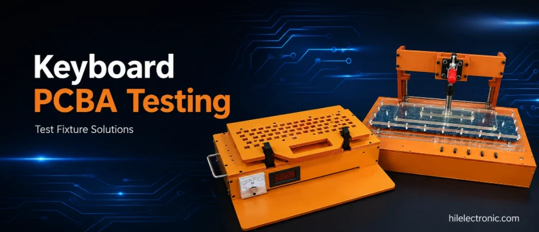
Keyboard PCBA Testing & Firmware Programming
Table of contentsKeyboard PCB Functional Testing Scope and...

Hall Effect Keyboard PCB Manufacturing & PCBA
Table of contentsHall Effect Keyboard PCB Buying...

ZMK Keyboard PCB Manufacturing & Assembly
Table of contentsZMK Wireless Keyboard PCBA Procurement...

Wireless Mechanical Keyboard PCB Manufacturing
Table of contentsWireless Keyboard PCB Procurement...
How to get a quote for PCBs
Let us run DFM/DFA analysis for you and get back to you with a report.
You can upload your files securely through our website.
We require the following information in order to give you a quote:
-
- Gerber, ODB++, or .pcb, spec.
- BOM list if you require assembly
- Quantity
- Turn time
In addition to PCB manufacturing, we offer a comprehensive range of electronic services, including PCB design, PCBA (Printed Circuit Board Assembly), and turnkey solutions. Whether you need help with prototyping, design verification, component sourcing, or mass production, we provide end-to-end support to ensure your project’s success. For PCBA services, please provide your BOM (Bill of Materials) and any specific assembly instructions. We also offer DFM/DFA analysis to optimize your designs for manufacturability and assembly, ensuring a smooth production process.