
Optimize PCB Layer Stackup: Materials, Impedance & EMI

Layer stackup isn’t merely a fabrication parameter—it’s the backbone of your PCB’s performance. The strategic vertical arrangement of signal, power, and ground layers directly influences signal integrity, EMC compliance, thermal stability, and production scalability.
At Highleap Electronics, we partner closely with engineers and procurement specialists, optimizing PCB layer stackups to ensure optimal performance, cost efficiency, reliable manufacturing, and long-term product success. This comprehensive guide highlights essential strategies and best practices—from conceptual planning to real-world manufacturing considerations.
1. Why Layer Stackup Makes or Breaks Your High-Speed PCB Design
Have you ever wondered:
Why do some PCBs pass EMI tests effortlessly, while others repeatedly fail despite identical schematics?
Often, the critical difference lies in the layer stackup.
The Three Essential Functions of Layer Stackup:
1. Ensuring Signal Integrity (SI)
Stackup defines impedance pathways. Improperly arranged layers lead to impedance mismatches, signal reflections, jitter, and EMI interference. High-speed signals require clear return paths via adjacent ground planes—a carefully planned stackup ensures exactly that.
2. Achieving Electromagnetic Compatibility (EMC)
EMC success hinges on effective field management. Good stackup design strategically confines electromagnetic fields between layers, creating low-inductance return paths and isolating sensitive signal and power domains, significantly reducing emissions and susceptibility.
3. Controlling Thermal Management
Ground and power layers act as thermal dissipators. Poorly designed stackups create thermal hotspots, particularly around high-power devices like regulators and transistors. A balanced layer arrangement ensures uniform heat dissipation and improved PCB reliability.
The most detailed schematic or layout can’t compensate for suboptimal stackup architecture. PCB performance—from high-frequency RF signals to sensitive USB differential pairs—depends fundamentally on the layer arrangement.
2. How to Engineer an Optimal Stackup: Actionable Guidelines for PCB Designers
Understand Electrical Intent Before Stackup Decisions
Designing an effective PCB stackup begins not with layer counts or copper weights, but with clear electrical intent. The stackup must support your performance envelope—not limit it. This starts by identifying critical parameters such as your highest signal frequency, impedance requirements (typically 50Ω single-ended or 100Ω differential), and whether your design integrates sensitive analog front-ends alongside noisy digital logic. These variables dictate trace geometry, plane strategy, and material selection. A failure to align stackup planning with electrical goals is one of the most common causes of EMI test failures, signal integrity degradation, and layout rework.
Once the electrical objectives are clarified, the next principle is proximity to reference planes. Every signal layer must be placed adjacent to a well-defined, uninterrupted return plane—typically ground. This enables low-inductance current return paths, which are essential for maintaining controlled impedance and preventing common-mode noise coupling. High-speed traces that lack a proper reference plane become antennas. Worse, transitions across split planes (e.g. under differential pairs) can introduce mode conversion, radiated EMI, and timing violations. Stackup isn’t just vertical structure—it’s field control.
Master Layer Pairing, Symmetry, and Materials
Beyond electrical behavior, mechanical symmetry in multilayer boards is crucial to manufacturability and long-term reliability. In stackups with more than four layers, copper and dielectric balance becomes a structural concern. Uneven distribution of copper weight or dielectric thickness leads to bowing, twisting, and lamination defects. Symmetrical layer mirroring—both in copper content and dielectric spacing—helps maintain flatness during press cycles, especially as temperature cycling and reflow stress compound over time. For high-layer-count boards, especially those in automotive, aerospace or industrial environments, this is non-negotiable.
Equally foundational is material selection. A well-chosen substrate determines not just impedance characteristics, but loss, thermal behavior, and production cost. Standard FR4 works well for general-purpose applications, but begins to suffer above 1–2 GHz due to its high dielectric loss (Df). For thermally stressed or high-speed applications, High-Tg FR4, Rogers 4350B, or Megtron 6 offer superior performance in terms of Dk stability, loss tangent, and process reliability. However, these materials introduce trade-offs in cost, layer bonding, and lamination temperature—engineering judgment is required to balance electrical benefit against fabrication feasibility.
Finally, no stackup should be finalized without proper impedance planning and manufacturing validation. At Highleap, we work directly with customers to define stackups that are not only optimized for signal performance and EMC, but also tailored to realistic fabrication capabilities. We provide detailed stackup proposals based on your electrical requirements, including dielectric materials, trace geometry, copper weights, and impedance targets—backed by real production tolerances and process insights. Relying on generic reference stackups is no longer sufficient at today’s speeds and densities. A production-ready stackup must be electrically accurate, mechanically reliable, and verified in collaboration with your PCB fabricator from the very beginning.

3. Real-World Insight: Transforming RF Sensor Performance through Stackup Redesign
To illustrate the critical importance of proper stackup design, here’s a real case from Highleap’s engineering archives—a project that moved from repeated EMI failures to full-volume production through precise layer architecture.
Project Overview
A European industrial technology startup was developing a high-frequency wireless sensor operating at 2.4 GHz, housed on an 8-layer PCB. The application was compact, densely populated, and RF-sensitive—yet despite a well-reviewed schematic and top-tier components, the prototype failed FCC EMI tests multiple times. The failures were not marginal; they were systematic, showing both radiated and conducted noise beyond acceptable thresholds.
Original Stackup Challenges
Upon review, the schematic looked sound. But the stackup told a different story:
- Lack of a dedicated RF reference plane: The RF traces were floating between poorly isolated internal layers, with inconsistent return paths and high loop inductance.
- Copper imbalance: Heavier copper pours on the top and bottom layers, with thin internal copper, created mechanical stress and warpage during reflow.
- Material mismatches: A high-Dk prepreg (intended for low cost) was selected without simulation, leading to uncontrolled impedance variation and signal skew.
- Routing congestion: Power and high-speed RF signals were sharing internal layers, introducing unintended coupling and field leakage.
In short, while the circuit logic was correct, the vertical layer strategy was electrically incoherent and mechanically unstable.
Highleap’s Stackup Solution
Our engineering team initiated a ground-up redesign of the layer stackup—not just adjustments, but a systematic architectural correction:
- Designed a symmetrical stackup structure, distributing copper weight evenly to eliminate lamination stress.
- Dedicated continuous ground reference planes directly below all RF layers, minimizing loop area and enabling controlled return current paths.
- Swapped the poorly matched dielectric for a hybrid build: Rogers 4350B in the RF path zones, combined with standard FR4 in non-critical areas—balancing electrical performance and cost.
- Using Polar Si9000, we simulated and tuned the microstrip and stripline geometries to achieve exact 100Ω differential impedance, factoring in real copper thickness and press-out data from our lamination process.
- The revised build included impedance test coupons and a full documentation package for traceability and design validation.
Outcomes
The impact of this engineering-led intervention was immediate and measurable:
- The revised prototype passed FCC EMI compliance on the first test cycle, with significant margin to spare.
- RF transmission metrics improved by over 18%, verified using a calibrated VNA in both time and frequency domains.
- The PCB exhibited no mechanical deformation, even after multiple thermal cycles, thanks to the balanced copper stackup.
- The design moved into 10,000-unit production without any further revision—reducing time-to-market and cutting development costs substantially.
Lesson Learned
This project underscores a fundamental truth in high-speed and RF PCB design:
Stackup isn’t an afterthought. It’s architecture.
No matter how refined your schematic or how expensive your components, a flawed stackup will sabotage signal integrity, fail compliance testing, and compromise reliability. Conversely, a well-engineered stackup—backed by simulation, material expertise, and process knowledge—can rescue an underperforming design and unlock successful mass production.
At Highleap, we treat stackup engineering not as a layout parameter, but as a core part of the electrical design strategy. That mindset consistently turns complex prototypes into scalable, compliant, and high-performance products.
4. Why Manufacturers Adjust PCB Stackups (And How to Avoid Surprises)
Using a Q&A format, let’s address frequent concerns engineers face regarding stackup adjustments by manufacturers:
Q: Why might a PCB manufacturer modify my stackup without notification?
A: Some factories do—but at Highleap, we believe transparency is essential. We always notify customers in advance and clearly explain any suggested modifications.
Q: What factors drive stackup adjustments during manufacturing?
- Material Availability: Specified dielectrics may temporarily run out, prompting selection of equivalent materials with matching electrical properties.
- Impedance Corrections: Adjustments to copper thickness or dielectric spacing to achieve exact impedance requirements.
- Balanced Lamination: Reducing the risk of PCB warpage by evenly distributing copper and dielectric layers.
- Yield Improvement: Enhancing fabrication consistency and registration accuracy for better yields.
Q: How can engineers avoid unexpected stackup modifications?
- Engage your PCB manufacturer during the design phase.
- Select widely stocked, standard materials whenever possible (we assist you with this).
- Request early-stage stackup validations (Highleap provides this service free of charge).
Q: What specific support does Highleap offer?
- Comprehensive impedance simulation and modeling
- Detailed stackup documentation with materials and tolerances clearly specified
- Thorough CAM and process engineering reviews
- Transparent communication and documented approval for any necessary revisions
- Continuous engineering support throughout layout and manufacturing stages
Conclusion
At Highleap Electronics, we believe that layer stackup is not a secondary parameter—it is the electrical and mechanical foundation upon which every successful PCB is built. Whether you’re developing a compact 4-layer board for consumer electronics or a complex, high-density 60-layer rigid-flex system for aerospace or datacenter hardware, the integrity of your design begins with how layers are planned, paired, and fabricated. A precisely engineered stackup governs signal performance, thermal behavior, EMC compliance, manufacturability, and long-term reliability—it is where design intent meets production reality.
To support your success, we provide a full suite of stackup-focused engineering services, including free consultation, impedance modeling, material system optimization, and controlled impedance validation with test coupons. Our capabilities extend to rigid and rigid-flex PCBs up to 60 layers, with integrated SMT, through-hole assembly, and engineering-led project management from prototype to mass production. Partner with Highleap to ensure your stackup isn’t just manufacturable—but performance-verified, production-scalable, and aligned with your product goals from the start.

Recommended Posts
PCB Trace Width Calculator: How to Size Traces for Current, Voltage Drop, and Impedance
Figure 1. A PCB trace width calculator is a starting point...
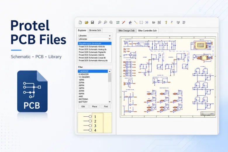
Protel PCB: Is It the Same as Altium Designer, and How to Open Legacy Protel Files
Figure 1. Legacy Protel PCB files often need review before...
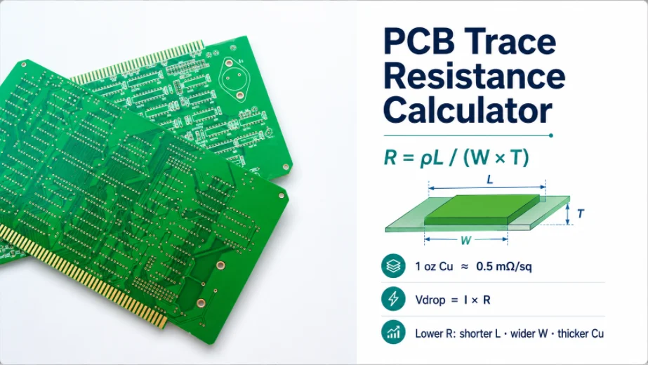
PCB Trace Resistance Calculator: How to Calculate Trace Resistance and Voltage Drop
Figure 1. PCB trace resistance affects voltage drop, heat...
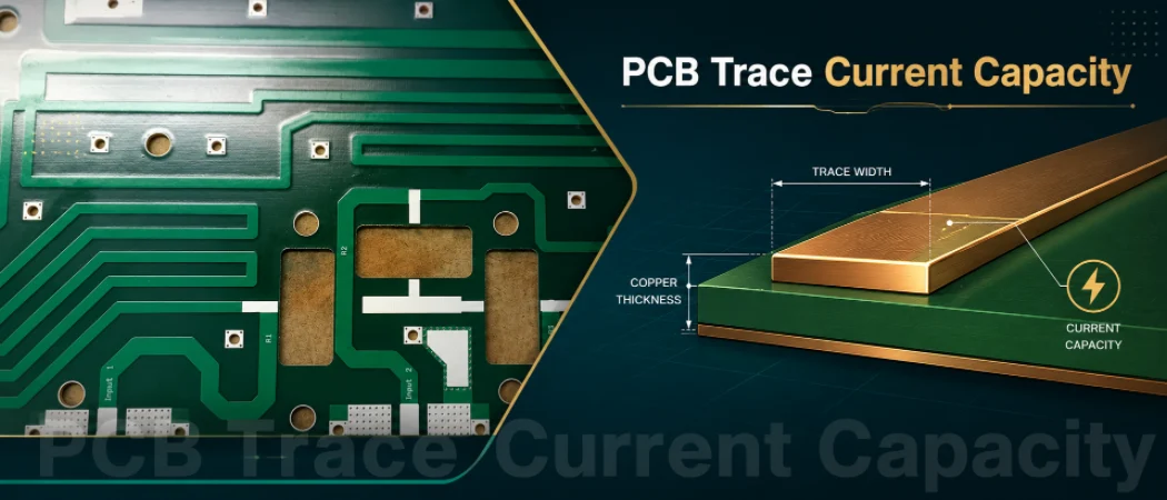
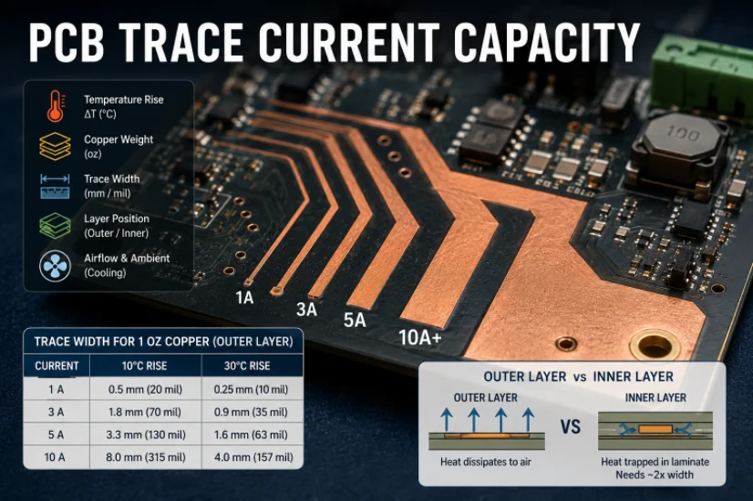
PCB Trace Current Capacity: Width, Copper Weight, and IPC-2221
Figure 1. PCB trace current capacity depends on copper...
How to get a quote for PCBs
Let‘s run DFM/DFA analysis for you and get back to you with a report. You can upload your files securely through our website. We require the following information in order to give you a quote:
-
- Gerber, ODB++, or .pcb, spec.
- BOM list if you require assembly
- Quantity
- Turn time
In addition to PCB manufacturing, we offer a comprehensive range of electronic services, including PCB design, PCBA, and turnkey solutions. Whether you need help with prototyping, design verification, component sourcing, or mass production, we provide end-to-end support to ensure your project’s success.
For PCBA services, please provide your BOM (Bill of Materials) and any specific assembly instructions. We also offer DFM/DFA analysis to optimize your designs for manufacturability and assembly, ensuring a smooth production process.