
Highleap Electronics: Reliable Charging Circuit PCB Manufacturing Solutions

At Highleap Electronics, we are a leading PCB manufacturer and assembly provider, delivering reliable charging circuit PCB solutions and innovative technologies for efficient battery charging systems, energy management, and power electronics. Our expertise spans across various industries, ensuring we meet diverse application requirements with precision and efficiency.
What is Charging Circuit PCB and Why is it Essential for Modern Charging Systems?
Charging circuit PCBs play a crucial role in modern battery charging systems, where they act as the backbone for controlling voltage, current, and charging phases. These PCBs are designed to manage complex power conversion processes while ensuring battery longevity and safety. As charging systems evolve, Charging circuit PCBs have become integral to achieving faster, safer, and more efficient charging solutions across applications ranging from portable devices to electric vehicles and renewable energy storage systems.
Key Features of Charging Circuit PCB for Fast Charging Solutions
The development of fast-charging technologies has led to a demand for highly specialized charging circuit PCBs capable of handling higher currents, improving efficiency, and maintaining safety standards. Key features include:
- High-Current Capability: Fast charging solutions require PCBs that can safely handle high currents. Our charging circuit PCBs are designed with heavy copper constructions that support high-current applications up to 500A, ensuring reliable operation even under maximum power conditions.
- Thermal Management Systems: Managing heat generation is critical for fast charging. Our PCBs include advanced thermal management solutions that dissipate heat efficiently, preventing thermal runaway and ensuring the safe operation of the system during rapid charging cycles. Integrated thermal sensors and heat sinks are employed to monitor and regulate temperature.
- High-Efficiency Power Conversion: Our charging circuit PCBs use advanced power conversion topologies to minimize energy losses during the charging process. These designs include high-efficiency DC-DC converters and precise regulation to ensure that power is transferred with minimal losses, leading to faster charging times and greater energy savings.
- Integration with Advanced Charging Protocols: The PCB supports modern charging standards, such as USB Power Delivery (USB-PD), which allows for dynamic voltage and current adjustments based on the device’s needs. This ensures that the charging process is optimized for each specific device, delivering maximum charging speed without compromising safety.
- Safety Features: Fast charging can be risky if not managed properly. Our charging circuit PCBs include multiple layers of safety features, including overcurrent protection, overvoltage protection, thermal protection, and short-circuit detection. These built-in safety mechanisms protect both the device and the battery during charging.
- Wireless Charging Support: With the rise of wireless charging technology, our PCBs are also designed to support inductive charging systems. These include features like resonant circuits that maximize energy transfer efficiency and minimize electromagnetic interference (EMI), ensuring smooth operation in wireless charging applications.
These features combine to offer reliable and efficient fast-charging solutions, ensuring that devices are charged quickly, safely, and with minimal energy loss.
Designing and Manufacturing High-Quality Charging Circuit PCBs
At Highleap Electronics, our expertise in PCB design and manufacturing guarantees the highest quality charging circuit PCBs. We employ advanced design techniques, including:
- Precision Analog Circuits: Our charging circuit PCBs feature ultra-low offset voltage and current measurement circuits, ensuring precise regulation and accurate monitoring of charging parameters.
- Heavy Copper Construction: We use heavy copper PCB materials to support high-current charging applications, ensuring that the PCB can handle the required power levels without overheating or damaging components.
- Advanced Thermal Solutions: We design our PCBs with embedded thermal management systems that use copper pours, heat sinks, and thermal vias to efficiently dissipate heat generated during fast charging operations.
- Customized Designs: Our PCB design process is tailored to each client’s specific application, whether it’s for electric vehicles, power banks, or renewable energy storage solutions, ensuring optimal performance and reliability.
We offer comprehensive PCB manufacturing services, including assembly, testing, and quality control, to meet the demanding requirements of charging systems.
Charging Circuit PCB Applications Across Various Industries
Charging circuit PCBs are used in a broad range of industries, each requiring specialized solutions to address unique charging challenges. Key applications include:
- Electric Vehicles (EVs): EV charging systems require high-efficiency charging circuits capable of handling large current flows. Our charging circuit PCBs integrate with Energy Storage PCBs to provide safe and efficient charging solutions.
- Portable Devices: Whether for smartphones, tablets, or laptops, our charging circuit PCBs enable fast and safe charging in portable electronic devices. The integration of Power Management IC PCBs ensures voltage stability during rapid charging cycles.
- Renewable Energy Systems: In solar and wind energy applications, our charging circuit PCBs work alongside Power Inverter PCBs to manage energy flow and optimize storage in energy systems.
- Data Centers: With increasing demand for efficient power management in data centers, our charging circuit PCBs ensure reliable power delivery to backup battery systems, supporting high-availability operations.

Seamless Integration of Charging Circuit PCBs with Power Management Systems
Charging circuit PCBs are not standalone components—they must work in harmony with various power management systems to optimize energy delivery and ensure safe charging operations. Integration with Energy Storage PCBs allows for intelligent energy management, ensuring that energy is stored and distributed efficiently. Furthermore, integration with Power Inverter PCBs enables bi-directional energy flow, ideal for vehicle-to-grid applications and renewable energy systems.
Fast Charging Technologies Supported by Charging Circuit PCBs
Our charging circuit PCBs are built to support the latest fast-charging technologies, enhancing the charging experience for consumers and businesses alike. These technologies include:
- USB Power Delivery (USB-PD): The USB Power Delivery protocol enables higher charging power levels up to 240W, allowing devices to charge faster while managing power efficiently.
- Qualcomm Quick Charge and MediaTek Pump Express: We integrate proprietary fast charging protocols into our PCBs, offering compatibility with a range of devices from various manufacturers.
- Wireless Charging: Inductive charging technology supports seamless power delivery without the need for physical connectors, ideal for charging pads, electric toothbrushes, and smartphones.
Testing and Validation of Charging Circuit PCBs
Our charging circuit PCBs undergo rigorous testing to ensure they meet performance, safety, and efficiency standards. Testing includes:
- Efficiency Testing: We measure the power conversion efficiency to ensure minimal energy loss during charging.
- Safety Validation: Each PCB is tested for overcurrent, overvoltage, and thermal protection to prevent hazards.
- EMC Testing: Electromagnetic compatibility (EMC) testing ensures that the PCBs perform without causing interference in sensitive environments.
These comprehensive tests ensure that every charging circuit PCB we produce is ready for real-world applications.
Why Choose Highleap Electronics for Advanced Charging PCB Solutions?
At Highleap Electronics, we pride ourselves on being a trusted leader in the PCB manufacturing and assembly industry, offering advanced, high-performance solutions for a wide range of applications. With years of expertise in designing and producing complex, multi-layer PCBs, we cater to industries like fast-charging systems, power electronics, and communication technologies. Our commitment to precision, efficiency, and innovation ensures that each PCB we produce meets the highest standards of quality and reliability.
Here’s why Highleap Electronics is your ideal partner for designing and manufacturing charging circuit solutions:
- Expertise in Fast-Charging Technologies: Our engineers are skilled in designing PCBs for fast-charging applications such as USB Power Delivery (USB-PD), Qualcomm Quick Charge, and wireless charging systems. We ensure seamless integration of the latest charging protocols into your product designs.
- Customized Solutions for Unique Needs: Every charging system has specific power, size, and performance requirements. Whether you’re developing electric vehicle charging stations, portable device chargers, or energy storage systems, we provide tailored solutions that meet your exact specifications.
- High-Precision Manufacturing Capabilities: Our advanced PCB fabrication facilities are equipped with cutting-edge tools and techniques to produce high-quality boards, from fine-pitch components to multi-layered designs and heavy copper constructions. This precision allows us to meet the demanding power and thermal management needs of modern charging solutions.
- Comprehensive Testing and Validation: We ensure that your charging PCBs perform safely and efficiently under real-world conditions. Our rigorous testing processes include thermal cycling, electromagnetic compatibility (EMC) testing, overcurrent protection, and efficiency analysis, ensuring compliance with industry standards.
- Commitment to Quality and Reliability: Quality control is a cornerstone of our manufacturing process. From material selection to final assembly, our quality assurance team performs thorough inspections to ensure every PCB meets the highest standards of reliability, ensuring long-term performance and reducing failure rates.
- Advanced Thermal Management Designs: Fast-charging systems generate significant heat, and our PCBs are designed with advanced thermal management solutions. These include heat sinks, copper pours, and thermal vias, all aimed at ensuring efficient heat dissipation and preventing overheating for long-lasting, safe operation.
- Complete Turnkey Services: We offer end-to-end solutions for your charging PCB needs. From design and prototyping to mass production and final assembly, we handle every aspect of the process, including supply chain management, to provide you with a one-stop shop for all your PCB requirements.
- Scalability for Global Markets: Whether you’re a startup or a multinational enterprise, we have the capacity to scale production to meet your needs. With global delivery capabilities, we efficiently support your projects from prototype to full-scale manufacturing, ensuring on-time delivery and cost-effective solutions.
With Highleap Electronics, you can trust that your charging circuit solutions will meet and exceed your performance, reliability, and innovation expectations. We are committed to the success of your fast-charging systems, energy management projects, and power electronics applications, ensuring you stay ahead with the latest and most efficient charging technologies available.
FAQs
Q: What charging current levels can your circuits support? Our designs support charging currents from as low as 100mA for small devices to up to 500A for electric vehicle fast charging.
Q: How do you ensure safe charging? Our Charging Circuit PCBs incorporate multiple safety features, including overvoltage, overcurrent, and thermal protection, ensuring safe charging across various battery chemistries.
Q: Do you offer wireless charging solutions? Yes, we offer advanced wireless charging solutions that comply with the Qi standard and can be customized to meet specific charging needs.
Q: How do you validate the performance of your PCBs? We perform a series of tests, including efficiency testing, safety validation, and thermal cycling to ensure our Charging Circuit PCBs meet industry standards.

Related Articles
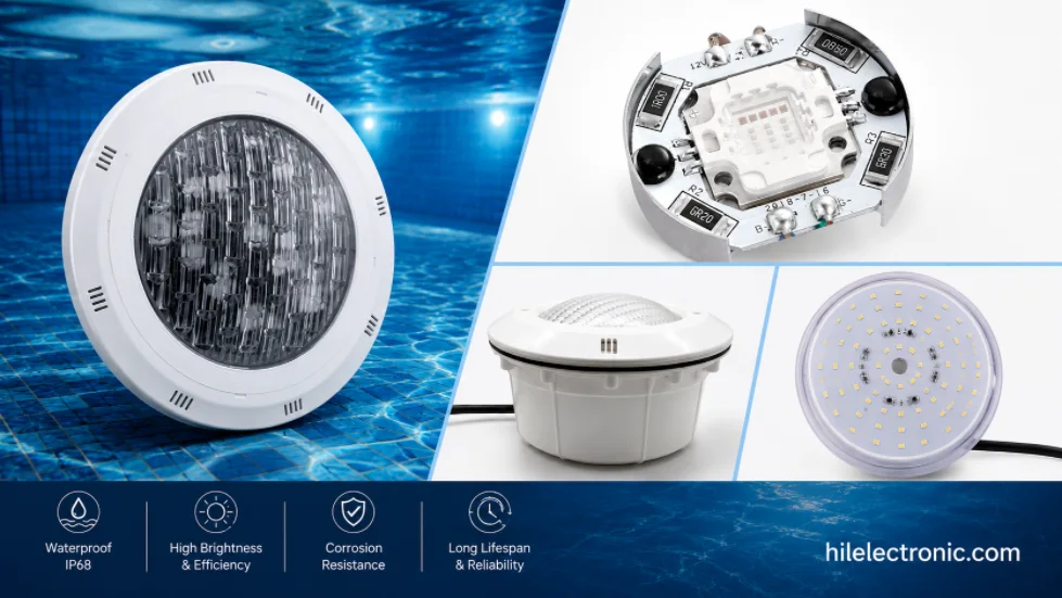
Underwater & Pool LED Light PCBs: IP68 Potted Boards, Low-Voltage Drivers & Safety
Figure 1. LED pool light PCB manufacturing reference....
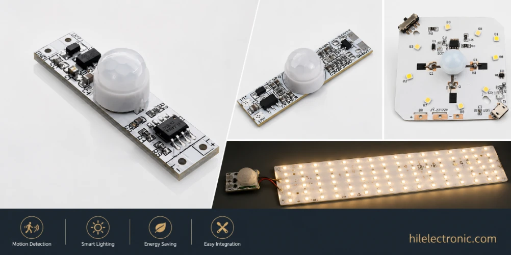
Motion Sensor & Smart LED Light PCBs: Sensor, Control, Driver & Wireless Boards
Figure 1. motion sensor LED light PCB manufacturing...
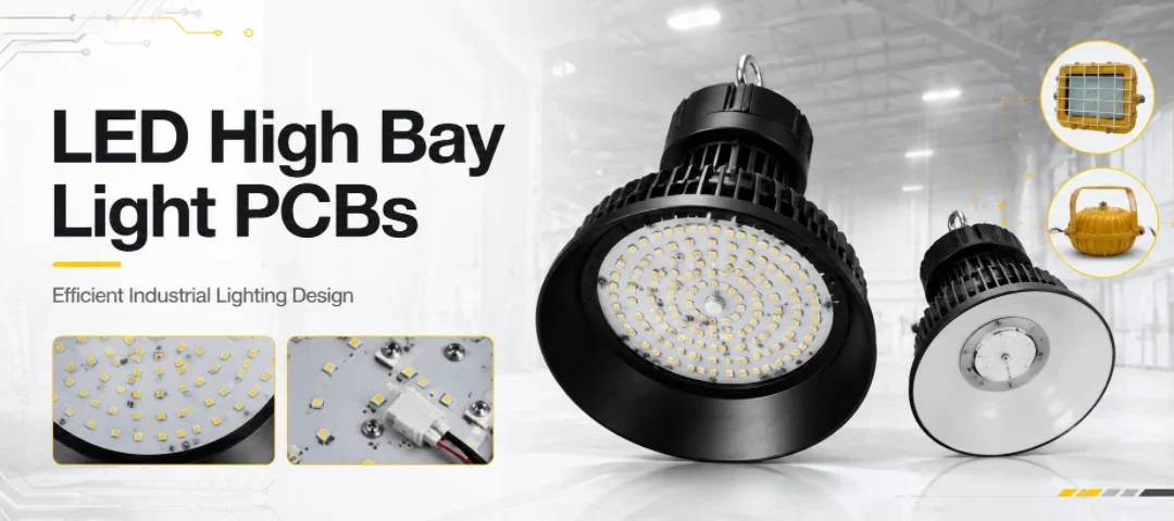
LED High Bay Light PCBs: Metal-Core Light Engines, Drivers & Turnkey Boards Built to Spec
Figure 1. LED high bay light PCB manufacturing reference....
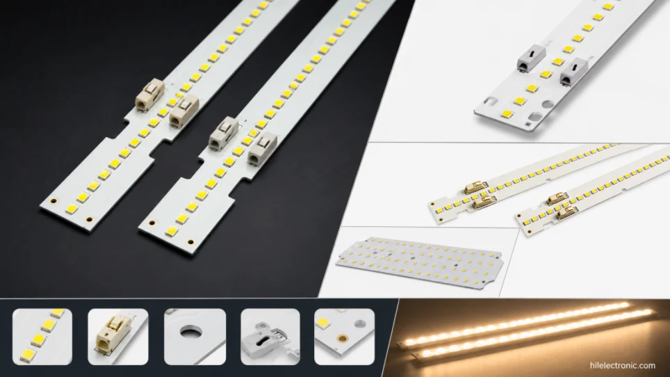
LED Linear & Strip Light PCBs: Long-Format Engines, Flexible & Rigid-Flex Boards
Figure 1. LED linear light PCB manufacturing reference....
How to get a quote for PCBs
Let us run DFM/DFA analysis for you and get back to you with a report.
You can upload your files securely through our website.
We require the following information in order to give you a quote:
-
- Gerber, ODB++, or .pcb, spec.
- BOM list if you require assembly
- Quantity
- Turn time
In addition to PCB manufacturing, we offer a comprehensive range of electronic services, including PCB design, PCBA (Printed Circuit Board Assembly), and turnkey solutions. Whether you need help with prototyping, design verification, component sourcing, or mass production, we provide end-to-end support to ensure your project’s success. For PCBA services, please provide your BOM (Bill of Materials) and any specific assembly instructions. We also offer DFM/DFA analysis to optimize your designs for manufacturability and assembly, ensuring a smooth production process.