
Challenges in Metal Core PCB Fabrication and How to Solve Them

Introduction
Metal Core Printed Circuit Boards (MCPCBs) have become indispensable in high-power LED lighting, automotive electronics, and power conversion systems due to their superior thermal management capabilities. However, MCPCB manufacturing challenges present significant complexities that differentiate this process from standard FR4 fabrication.
The fundamental difference lies in bonding copper circuitry to metal substrates—typically aluminum or copper—through specialized dielectric layers, creating unique thermal, mechanical, and processing difficulties. These challenges stem from material property mismatches, stringent flatness requirements, and the demanding thermal environments these boards must withstand.
This article examines the primary obstacles encountered during metal core PCB fabrication and presents practical engineering solutions that ensure consistent quality and performance.
Thermal Expansion Mismatch: A Critical MCPCB Manufacturing Challenge
Understanding the Challenge
A major MCPCB manufacturing challenge is managing thermal expansion mismatch among the aluminum base, copper foil, and dielectric layer. Their different coefficients of thermal expansion (CTE)—about 23 ppm/°C for aluminum, 17 ppm/°C for copper, and 30–80 ppm/°C for dielectrics—generate internal stress during heating and cooling.
During lamination above 150 °C, these CTE differences cause delamination, dielectric cracking, or board deformation. Fast heating or thick metal layers intensify stress, while repeated thermal cycling gradually weakens interlayer adhesion, leading to long-term reliability issues.
Practical Solutions
-
CTE-Matched Dielectrics – Choose dielectric materials with CTE values between copper and aluminum. Ceramic-filled dielectrics offer balanced expansion and high thermal conductivity (≥2 W/m·K).
-
Controlled Lamination Profile – Use a 2–3 °C/min temperature ramp with adequate dwell time for stress relaxation before cooling.
-
Balanced Thickness Ratio – Keep the copper-to-metal base thickness ratio between 1:10 and 1:15 to distribute stress evenly.
-
Symmetrical Circuit Design – Maintain balanced copper distribution to minimize deformation during thermal cycling.
These combined strategies effectively reduce CTE-related failures and improve MCPCB reliability.

PCB Warpage
Warpage Control in MCPCB Manufacturing Challenges
The Warpage Problem
Warpage control is another critical MCPCB manufacturing challenge, especially in boards larger than 200 mm. Even a 0.5 mm deviation can affect SMT placement accuracy and create air gaps that reduce thermal transfer to heatsinks.
Asymmetric designs with uneven copper distribution between layers are the main cause. When one side carries dense circuitry and the other remains bare, differential shrinkage during cooling leads to bowing. Inconsistent lamination pressure or insufficient cushioning in vacuum presses further increases residual stress, resulting in warpage after cooling.
Effective Solutions
- Symmetric Stackup Design – Use balanced copper distribution on both sides of the dielectric layer to equalize contraction forces during thermal processing.
- Compensating Copper Patterns – For asymmetric layouts, add non-functional copper areas or mesh on the opposite side to maintain structural balance.
- Controlled Lamination Pressure – Maintain pressure around 15–25 kg/cm² and cooling rates below 3 °C/min to prevent stress locking.
- Post-Lamination Annealing – Apply stress-relief annealing at temperatures 20–30 °C below the dielectric’s glass transition point to improve flatness stability.
- Fixture-Assisted Flattening – Use mechanical fixtures during final curing to achieve flatness within 0.3 mm per 100 mm of board length.
These measures effectively minimize warpage and ensure mechanical stability throughout the MCPCB manufacturing process.
Lamination and Dielectric Integrity in MCPCB Manufacturing
Dielectric Cracking Challenges
Lamination defects and dielectric cracking are major MCPCB manufacturing challenges that affect both insulation reliability and heat transfer efficiency. Cracks often originate near board edges or through-holes, forming potential paths for electrical breakdown.
Even small delamination areas create air gaps with thermal resistance up to 100 times higher than bonded regions, causing localized hotspots that accelerate component failure. Common causes include poor resin flow, low glass transition temperature (Tg) materials, or moisture trapped within the dielectric layer.
Preventive Approaches
- High-Tg Dielectrics – Use materials with Tg above 150 °C to maintain dimensional stability and withstand repeated thermal cycling.
- Optimized Lamination Pressure – Begin with low pressure to promote resin flow, then gradually increase to full bonding pressure for uniform adhesion.
- Pre-Baking for Moisture Removal – Bake dielectric sheets at 120 °C for 2–4 hours before lamination to eliminate absorbed moisture.
- Vacuum-Assisted Lamination – Employ vacuum systems to remove trapped air and volatiles, ensuring void-free bonding and consistent thermal performance.
These preventive measures improve dielectric reliability and ensure stable thermal performance in metal core PCB manufacturing.
Drilling and Routing Challenges in MCPCB Manufacturing
Mechanical Processing Difficulties
The hardness and high thermal conductivity of metal substrates create distinct MCPCB manufacturing challenges during drilling and routing. Aluminum bases with Brinell hardness values of 40–80 HB quickly wear standard carbide drill bits, resulting in oversized holes, rough walls, and poor plating adhesion.
Metal burrs or chips generated during processing may cause short circuits or interfere with component placement. Because aluminum and copper efficiently dissipate heat, the cutting zone remains hard while the drill heats through friction, accelerating tool wear and dimensional inaccuracy.
Optimized Drilling Solutions
- Specialized Drill Tools – Use polycrystalline diamond (PCD) or coated carbide bits to extend tool life 10–20× compared to standard drills.
- Optimized Drilling Parameters – Operate at 40,000–60,000 RPM with feed rates of 50–100 mm/min to balance precision and wear control.
- Proper Support Materials – Apply phenolic or aluminum entry and backup boards for cleaner hole entry and exit.
- Peck Drilling Cycles – Use intermittent drilling to clear chips and reduce thermal buildup.
- Precision Routing – Choose compression-style end mills with suitable flute geometry to minimize edge tearing and burrs.
These machining strategies improve hole quality, extend tool life, and ensure dimensional accuracy in metal core PCB fabrication.

Surface Treatment Challenges in MCPCB Manufacturing
Oxidation and Contamination Issues
Metal core surfaces oxidize quickly when exposed to air, especially under elevated processing temperatures. Aluminum forms oxide layers that hinder solder wetting, while copper develops cuprous and cupric oxides that degrade electrical contact and bonding strength. These MCPCB manufacturing challenges demand immediate surface protection to preserve assembly reliability.
Protection Strategies
- Timely Surface Finishing – Apply protective coatings immediately after fabrication to prevent oxidation during handling and storage.
- ENIG Finish – Use Electroless Nickel Immersion Gold for excellent solderability and long shelf life exceeding 12 months.
- OSP Coating – Choose Organic Solderability Preservatives as a cost-effective option for short-term protection.
- Cleanliness Control – Rinse with deionized water to remove ionic residues that can accelerate corrosion.
- Moisture-Proof Packaging – Store boards in vacuum-sealed packaging with desiccants to protect against oxidation.
Implementing rapid post-fabrication finishing and proper packaging practices ensures stable solderability and long-term reliability in metal core PCB manufacturing.
Quality Control and Testing in MCPCB Manufacturing Challenges
Inspection Complexities
MCPCB quality inspection requires specialized testing methods beyond standard PCB evaluation. Thermal resistance testing must accurately assess heat transfer from the circuit layer to the metal base under controlled thermal conditions.
Dielectric breakdown testing confirms insulation strength at voltages above operating levels, while flatness inspection demands micron-level precision to ensure proper thermal contact. These factors make quality verification one of the major MCPCB manufacturing challenges.
Comprehensive Testing Solutions
Effective MCPCB quality control involves multiple complementary verification processes:
- Thermal Resistance Testing – Validate heat conductivity using calibrated sensors, maintaining values typically below 1 °C/W for standard designs.
- High-Potential Testing – Apply 2500–3000 VAC to ensure dielectric integrity and insulation reliability.
- Infrared Thermal Imaging – Detect hotspots that indicate poor thermal transfer or hidden circuit anomalies.
- Laser-Based AOI Inspection – Measure surface flatness with high precision to identify warpage before assembly.
Implementing statistical process control with regular sampling maintains production stability and ensures consistent performance across all MCPCB manufacturing stages.
Conclusion
Overcoming MCPCB manufacturing challenges—from thermal expansion mismatches and warpage control to drilling precision and surface protection—requires a holistic engineering approach. Success depends on aligning material selection, process optimization, and quality control to ensure stable thermal performance and long-term reliability in high-power applications.
Why Choose Highleap Electronics
- Advanced Material Engineering – Tailored aluminum, copper, and dielectric selections for balanced thermal and mechanical performance.
- Precision Process Control – Optimized lamination, drilling, and routing parameters for superior flatness and dimensional accuracy.
- Comprehensive Quality Assurance – In-house thermal resistance, dielectric, and flatness testing to verify every production batch.
- Application Expertise – Proven performance across LED lighting, automotive systems, and power conversion industries.
Partner with Highleap Electronics to access optimized MCPCB manufacturing solutions engineered for performance, reliability, and scalability. Contact our technical team today to discuss your high-power project requirements.

Recommended Posts
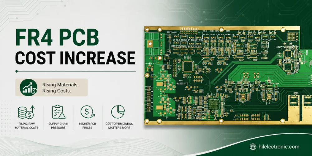
FR4 PCB Cost Increase for Electronics Manufacturers
Table of contents Why FR4 Prices Continue to Rise Raw...
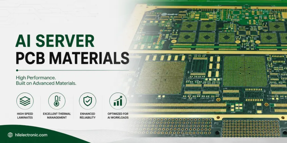
AI Server PCB Materials: Low-Loss Laminates, Stack-Up, Thermal and PCBA Guide
On this page What AI Server PCB Materials Need to Solve...
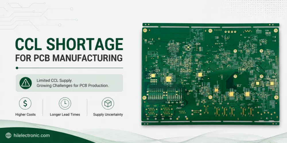
CCL Shortage for PCB Manufacturing
On this page Why Copper Clad Laminate Availability Matters...
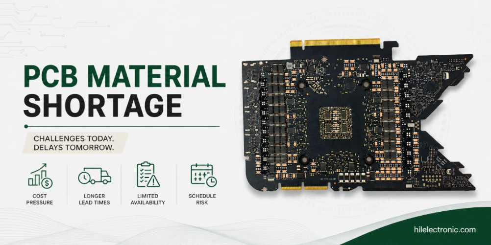
PCB Material Shortage Impact on Cost and Lead Time
On this page Why PCB Material Shortages Continue to Affect...
How to get a quote for PCBs
Let‘s run DFM/DFA analysis for you and get back to you with a report. You can upload your files securely through our website. We require the following information in order to give you a quote:
-
- Gerber, ODB++, or .pcb, spec.
- BOM list if you require assembly
- Quantity
- Turn time
In addition to PCB manufacturing, we offer a comprehensive range of electronic services, including PCB design, PCBA, and turnkey solutions. Whether you need help with prototyping, design verification, component sourcing, or mass production, we provide end-to-end support to ensure your project’s success.
For PCBA services, please provide your BOM (Bill of Materials) and any specific assembly instructions. We also offer DFM/DFA analysis to optimize your designs for manufacturability and assembly, ensuring a smooth production process.