
MCPCB Via Design | Engineering Thermal Pathways for High-Power Applications

Introduction: MCPCB Via Design Fundamentals in Heat Management
In Metal Core PCBs, vias serve not only as electrical interconnects but also as essential thermal pathways, transferring heat from surface-mounted components to the underlying aluminum or copper substrate. The design and placement of thermal vias directly impact junction temperatures in high-power LEDs and the safe operation of power modules.
Modern high-performance applications—such as automotive LED headlights, industrial converters, and RF amplifiers—depend on optimized via configurations to ensure reliable thermal management. Effective MCPCB via design balances heat dissipation, electrical isolation, and manufacturability, enabling engineers to extend product lifetime and maintain performance under demanding conditions.
Types of Vias in MCPCB Via Design Applications
Signal Vias
Signal vias in MCPCB via design ensure reliable electrical connectivity between circuit layers while traversing the dielectric barrier. Key design factors include precise via diameter, insulation distance, and compliance with voltage clearance requirements:
- Diameter control – Typically 0.2mm to 0.5mm to maintain impedance matching and signal integrity
- Insulation spacing – Minimum 0.25mm for applications up to 250V AC; 0.5mm or greater for higher voltages
- Electrical safety – Clearance and barrel insulation prevent shorting during thermal cycling
Thermal Vias
Thermal vias create dedicated heat dissipation paths from component pads to the metal core, maximizing thermal conductivity and reducing junction temperature. Design considerations include via size, density, and placement:
- Via diameter – Larger than signal vias, typically 0.3mm to 1.0mm
- Via density – Higher density arrays under high-power components enhance heat transfer
- Array layout – Optimized to match heat flux distribution and achieve thermal resistances below 1.5°C/W in typical LED applications
Blind and Buried Vias in Multilayer MCPCB
Blind and buried vias enable selective layer interconnection in multilayer MCPCBs, maintaining thermal pathway integrity while allowing high component density. Key design aspects include:
- Layer-specific connection – Blind vias connect top layers to internal layers without penetrating the full board thickness
- Thermal separation – Separates signal routing from thermal management paths for complex power systems
- Precision manufacturing – Requires accurate drilling depth and layer registration
Filled or Plugged Vias
The filling material selection in MCPCB via design significantly impacts thermal performance and assembly reliability. Three primary options dominate the industry:
- Copper-filled vias – Maximum thermal conductivity at 385 W/m·K enables superior heat transfer for extreme power applications
- Silver-filled epoxy – Balanced cost-performance at 15-60 W/m·K conductivity suitable for moderate power designs
- Thermally conductive resin – Cost-effective solution at 2-8 W/m·K preventing solder wicking while maintaining acceptable thermal performance
Critical MCPCB Via Design Thermal Considerations
Via Diameter and Density Optimization
Via diameter and array density jointly determine total thermal conductance in MCPCB via design. Smaller vias (0.3–0.4mm) support high-density arrays, while larger vias (0.8mm) improve individual thermal conductance but limit packing. Optimal configurations balance heat spreading with manufacturability:
- Small-diameter vias – High-density arrays (100–120 vias/cm²) enhance lateral heat distribution
- Large-diameter vias – Lower density (20–30 vias/cm²) but better single-via conduction
- Example – 0.4mm vias spaced 1.0mm apart reduce junction-to-case thermal resistance by 40–60%
Via Arrangement and Layout Patterns
Strategic placement of thermal vias maximizes heat transfer beneath high-power components:
- Direct alignment – Vias centered under thermal pads or heat slugs
- Array patterns – Hexagonal arrays provide up to 15% better thermal performance than rectangular grids
- Component-specific layout – LED: 3×3 or 4×4 arrays; Power semiconductors: dense clusters under die attach areas
Dielectric Layer Thickness Impact
Dielectric thickness and material define the thermal resistance between component and metal core:
- Standard thickness – 75–200μm, thermal conductivity 1–3 W/m·K
- Premium dielectrics – Ceramic-filled, 5–8 W/m·K, higher cost
- Design impact – Each 25μm increase in thickness adds ~0.3–0.5°C/W thermal resistance; must balance heat dissipation and electrical isolation, especially >600V applications
Advanced MCPCB Via Filling and Plating Techniques
Copper-Filled Via Implementation
Copper-filled vias provide the highest thermal performance in MCPCB via design, with conductivity up to 385 W/m·K. Electroplating fills via barrels completely, eliminating air voids that reduce heat transfer. This method suits high-power and high-reliability applications:
- Thermal advantage – Void-free copper maximizes heat dissipation
- Processing – Specialized pulse plating; 0.5mm vias require 3–5 hours for complete filling
- Quality control – Cross-sectional inspection ensures <5% voids; higher void content reduces conductivity by 15–20%
Conductive Epoxy and Resin Solutions
Thermally conductive epoxies and resins offer cost-effective alternatives for moderate-power MCPCB via design applications:
- Silver-loaded epoxy – 15–60 W/m·K, excellent adhesion and thermal cycle resistance
- Aluminum-filled compounds – 3–10 W/m·K, suitable for consumer electronics
- Ceramic-filled resins – 2–5 W/m·K, electrically insulative for isolation-critical applications
These materials prevent solder wicking and allow rapid via filling via screen printing, reducing production time compared to copper electroplating.
Via Surface Treatments and Capping
Surface treatments enhance assembly reliability while maintaining thermal performance in MCPCB via design:
- Solder mask tenting – Prevents solder infiltration; mask thickness ≤20μm to limit added thermal resistance
- Plated via caps – ENIG or immersion silver finishes provide solderable surfaces while sealing vias; typical plating thickness 3–5μm
- Selective plating – Keeps thermal vias open if post-assembly filling is needed, while protecting signal vias

Metal Core PCB
Optimized MCPCB Via Design Implementation Strategies
Effective thermal management in MCPCB via design requires coordinated layout, simulation, and manufacturing planning. Key implementation strategies include:
- Thermal via placement – High-density arrays positioned directly beneath power components, extending 2–3mm beyond component outlines to enhance lateral heat spreading
- Thermal simulation – Validate junction temperatures, via thermal resistance, and substrate spreading resistance before production; target at least 25°C below maximum ratings for reliability
- Manufacturing constraints – Mechanical drilling supports 0.2mm minimum holes; laser drilling enables 0.1mm microvias for ultra-dense arrays
- Aspect ratio considerations – Drill depth-to-diameter ratio ≤10:1 for reliable plating; filled vias typically <1:1 to ensure void-free electroplating
Manufacturing Excellence and Reliability in MCPCB Via Design
Drilling method selection impacts both quality and cost in metal core PCB via design implementation. Mechanical drilling provides consistent hole quality for diameters above 0.25mm, with positional accuracy within ±0.05mm. This precision suits most thermal management applications where via placement tolerances align with standard PCB manufacturing capabilities.
Laser drilling excels for high-density MCPCB via design arrays with holes below 0.2mm diameter. UV laser systems minimize heat-affected zones to under 20μm, preventing dielectric degradation. CO₂ lasers offer faster processing but require careful parameter control to prevent excessive carbonization.
Thermal Cycling and Reliability Testing
Thermal cycling reliability in MCPCB via design depends critically on via structure integrity and filling quality. Key factors affecting long-term performance include:
- CTE mismatch management – Copper (17 ppm/°C) versus aluminum substrate (23 ppm/°C) creates cyclical stress requiring proper via design
- Via wall thickness – Minimum 20μm copper plating withstands repeated thermal excursions without barrel cracking
- Fill material integrity – Properly filled vias distribute stresses more effectively than hollow vias, extending lifetime by 2-3×
Quality verification through automated optical inspection confirms proper MCPCB via design execution. Cross-sectional analysis validates filling completeness and plating uniformity. Thermal resistance measurements using transient thermal analysis verify manufactured boards meet specifications.
Conclusion: Excellence in MCPCB Via Design for Thermal Management
MCPCB via design is critical for effective thermal management in high-power electronics. Properly sized, positioned, and filled thermal vias create low-resistance pathways that keep component temperatures within safe limits, enabling higher power densities and long-term reliability. Advanced materials, precise MCPCB manufacturing, and thermal simulation further enhance via performance, making optimized designs essential for applications from automotive LEDs to 5G infrastructure.
Highleap Electronics Capabilities in MCPCB Via Design:
- Precision via drilling – Mechanical and laser drilling for microvias and high-density arrays
- Via filling solutions – Copper, silver-filled epoxy, and thermally conductive resin options for tailored thermal performance
- Surface treatments & plating – ENIG, immersion silver, and solder mask tenting to ensure reliability and assembly quality
- Design support & thermal validation – Collaboration on layout, via placement, and thermal simulation to optimize heat dissipation

Recommended Posts
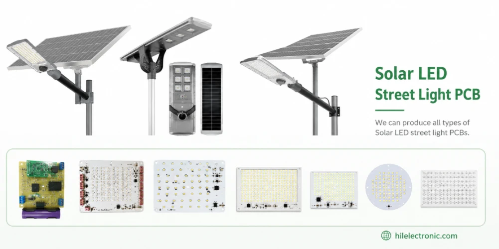
Solar LED Street Light PCB: Charge Controllers, BMS & Light Engines
Figure 1. Solar LED street light PCB product architecture...
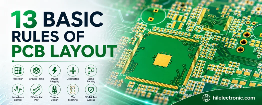
13 Basic Rules of PCB Layout (and the Failures They Prevent)
Figure 1. 13 Basic Rules Of Pcb Layout reference image for...

PCB Current Calculator: Sizing Trace Width and Vias with the IPC-2221 Formula
Figure 1. Pcb Current Calculator reference image for PCB...

Microphone PCB Design: How the Board Itself Shapes Your Audio Quality
Figure 1. Microphone Pcb reference image for PCB...
How to get a quote for PCBs
Let‘s run DFM/DFA analysis for you and get back to you with a report. You can upload your files securely through our website. We require the following information in order to give you a quote:
-
- Gerber, ODB++, or .pcb, spec.
- BOM list if you require assembly
- Quantity
- Turn time
In addition to PCB manufacturing, we offer a comprehensive range of electronic services, including PCB design, PCBA, and turnkey solutions. Whether you need help with prototyping, design verification, component sourcing, or mass production, we provide end-to-end support to ensure your project’s success.
For PCBA services, please provide your BOM (Bill of Materials) and any specific assembly instructions. We also offer DFM/DFA analysis to optimize your designs for manufacturability and assembly, ensuring a smooth production process.