
DBC Process for Ceramic Substrate Manufacturing

The DBC (Direct Bonded Copper) process creates a permanent metallurgical bond between copper and ceramic through controlled high-temperature oxidation. Understanding this manufacturing process enables engineers to specify substrates that meet reliability requirements and helps procurement teams evaluate supplier capabilities.
Table of Contents
At Highleap Electronics, we follow controlled DBC manufacturing processes and consistent quality standards to ensure stable substrate performance for power electronics applications. This guide outlines the fundamental principles of DBC processing and is intended to help engineers better understand process requirements, define appropriate specifications, and evaluate suppliers with greater confidence.
1) Overview of the DBC Process
The DBC process represents a specialized manufacturing technique for creating DBC substrates—ceramic circuit boards with copper conductors bonded directly to the ceramic surface without intermediate adhesives. Developed in the 1970s, this process has become the standard method for producing high-performance substrates for power electronics.
Unlike conventional PCB fabrication that relies on mechanical or adhesive bonding, the DBC process creates a chemical bond at the copper-ceramic interface. This bond forms through a carefully controlled reaction involving copper oxide as an intermediate phase, resulting in exceptional bond strength and thermal conductivity.
The process requires specialized equipment including high-temperature furnaces capable of precise atmosphere control, clean room facilities for contamination-sensitive steps, and inspection systems to verify bond quality. These requirements distinguish DBC manufacturing from standard electronics production.
2) Principle of Direct Copper-to-Ceramic Bonding
The fundamental principle underlying DBC technology involves forming a copper oxide layer at the copper-ceramic interface that reacts with both materials to create a permanent bond. This occurs at temperatures near the copper-oxygen eutectic point (1065°C).
2.1 The Bonding Mechanism
When copper foil contacts ceramic at elevated temperatures in a controlled oxygen atmosphere, the following sequence occurs:
- Surface oxidation: Copper at the interface oxidizes to form Cu₂O (cuprous oxide)
- Eutectic formation: At approximately 1065°C, copper and cuprous oxide form a eutectic liquid at the interface
- Ceramic wetting: The liquid phase wets and penetrates the ceramic surface
- Solidification: Upon cooling, the interface solidifies, creating a strong metallurgical bond
For alumina (Al₂O₃) ceramics, the bond forms through a combination of mechanical interlocking and chemical reaction between copper oxide and the ceramic surface. With aluminum nitride (AlN), additional surface preparation may be required since AlN’s native oxide layer can interfere with bonding.
2.2 Critical Process Parameters
- Temperature: Must be precisely controlled within ±2°C to ensure proper eutectic formation without excessive copper melting
- Oxygen partial pressure: Controls oxide layer thickness; too little prevents bonding, too much causes excessive oxidation
- Time at temperature: Sufficient for complete wetting but not so long as to cause grain growth in copper
- Cooling rate: Affects residual stress and potential for ceramic cracking
3) Key Manufacturing Stages
DBC substrate manufacturing follows a defined sequence of processing steps, each critical to final product quality. Understanding these stages helps engineers and buyers evaluate supplier capabilities.
3.1 Material Preparation
- Ceramic inspection: Incoming ceramic substrates are inspected for surface defects, flatness, and contamination
- Copper preparation: Oxygen-free copper foil is inspected and cleaned to remove oils and surface oxides
- Surface treatment: Some ceramics, particularly AlN, require surface oxidation or other treatments before bonding
3.2 Bonding
- Stack assembly: Copper foil is positioned on one or both sides of the ceramic substrate
- Furnace loading: Assemblies are loaded into high-temperature furnaces with controlled atmosphere capability
- Thermal profile execution: Precise temperature ramps, holds, and cooling profiles are executed according to the ceramic type
- Post-bond inspection: Visual and ultrasonic inspection verifies bond integrity
3.3 Circuit Patterning
- Photoresist application: Photosensitive resist is laminated or coated onto the copper surface
- Exposure and development: Circuit patterns are transferred using photolithography
- Copper etching: Unwanted copper is removed using ferric chloride or cupric chloride etchants
- Resist stripping: Remaining photoresist is removed, leaving the copper circuit pattern
3.4 Surface Finishing
- Nickel plating: Provides oxidation protection and solderable surface
- Gold plating: Applied for wire bondable surfaces or enhanced corrosion resistance
- Silver plating: Used for sintered silver die attach applications
3.5 Singulation and Final Processing
- Laser scribing: Ceramic is scored to create break lines for individual substrates
- Breaking or cutting: Individual substrates are separated along scribe lines
- Final inspection: Dimensional verification, visual inspection, and electrical testing
- Packaging: Substrates are packaged in ESD-safe containers with moisture protection
4) Process Challenges and Control Points
DBC manufacturing presents unique challenges that require careful process control. Understanding these challenges helps specify appropriate quality requirements.
4.1 Bond Void Formation
Voids at the copper-ceramic interface reduce thermal conductivity and can cause localized hot spots under power devices. Causes include contamination, insufficient atmosphere control, and improper temperature profiles. Quality manufacturers use scanning acoustic microscopy (SAM) to detect and quantify bond voids, typically specifying maximum void percentage (e.g., <2% total area).
4.2 Ceramic Cracking
The CTE mismatch between copper and ceramic creates thermal stress during cooling. If cooling is too rapid or non-uniform, the ceramic may crack. Process optimization balances cooling rate to minimize stress while maintaining productivity. Ceramic thickness and copper thickness ratio also affects cracking tendency.
4.3 Surface Finish Quality
Power device assembly requires precise surface finish specifications for reliable die attach and wire bonding. Plating thickness, uniformity, and contamination control directly affect downstream assembly yields. Critical parameters include plating thickness tolerance, surface roughness, and cleanliness.
4.4 Dimensional Control
High-temperature processing can cause warpage and dimensional changes. Specifications for flatness (typically <0.1mm per 25mm), dimensional tolerance, and registration between copper patterns and ceramic features require careful process control throughout manufacturing.
5) Reliability and Thermal Cycling Performance
DBC substrate reliability under thermal cycling is critical for power electronics applications. The bonding process parameters directly influence long-term reliability performance.
5.1 Thermal Cycling Mechanisms
During thermal cycling, the CTE difference between copper and ceramic creates cyclic stress at the interface. Over many cycles, this stress can cause fatigue cracks to initiate at the copper-ceramic boundary, eventually propagating through the bond. Failure modes include delamination, copper cracking, and ceramic fracture.
5.2 Factors Affecting Thermal Cycling Life
- Copper thickness: Thicker copper increases stress; optimal thickness balances current handling against reliability
- Temperature swing: Larger ΔT accelerates fatigue; -40°C to +150°C is more demanding than 0°C to +100°C
- Ceramic material: Si₃N₄ offers superior thermal cycling performance due to higher fracture toughness
- Bond quality: Voids and weak bonds accelerate failure
- Circuit geometry: Sharp corners and narrow gaps concentrate stress
5.3 Testing Standards
Thermal cycling reliability is typically verified according to industry standards such as AQG 324 (automotive qualification) or customer-specific test protocols. Common test conditions include temperature swings from -40°C to +125°C or -55°C to +150°C, with cycle counts ranging from 1,000 to 5,000+ depending on application requirements.
6) How the DBC Process Impacts Final Substrate Quality
Every step in the DBC manufacturing process influences the quality and performance of the finished substrate. When evaluating suppliers or specifying substrates, consider how process capabilities affect:
- Thermal performance: Bond void content directly affects thermal resistance; specify maximum void percentage
- Electrical reliability: Ceramic quality and processing affect partial discharge performance at high voltages
- Assembly yield: Surface finish quality impacts die attach and wire bonding success rates
- Long-term reliability: Bonding process parameters determine thermal cycling lifetime
Highleap Electronics maintains rigorous process controls throughout DBC manufacturing. Our facilities include advanced inspection equipment for bond void detection, dimensional verification, and surface quality analysis. For detailed information about our ceramic PCB capabilities, or to discuss your specific requirements, our engineering team is ready to assist.
Learn more about selecting the right ceramic material in our DBC ceramic substrate guide, or explore prototyping options at our DBC substrate prototype service page.
For a comprehensive overview of DBC technology and applications, visit our DBC substrate hub page, or learn more about the terminology at our direct bonded copper substrate definition page.

Recommended Posts
EAGLE PCB Software: Is It Free, EAGLE vs KiCad, and How to Export Gerber Files
Figure 1. EAGLE PCB software projects should be exported...
Microcontroller Board Soldering and Programming: QFN Pads, SWD, and FTDI Drivers
Figure 1. Microcontroller board soldering and programming...
Solder Paste for SMT Assembly: Types, Storage, and Printing Defects
Figure 1. Solder paste selection affects SMT print...
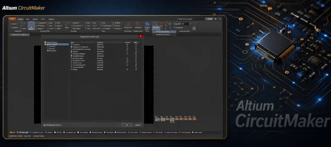
Altium CircuitMaker: Is It Free, How Does It Compare, and How to Export Gerbers for Manufacturing
Figure 1. Altium CircuitMaker files should be checked...
How to get a quote for PCBs
Let us run DFM/DFA analysis for you and get back to you with a report.
You can upload your files securely through our website.
We require the following information in order to give you a quote:
-
- Gerber, ODB++, or .pcb, spec.
- BOM list if you require assembly
- Quantity
- Turn time
In addition to PCB manufacturing, we offer a comprehensive range of electronic services, including PCB design, PCBA (Printed Circuit Board Assembly), and turnkey solutions. Whether you need help with prototyping, design verification, component sourcing, or mass production, we provide end-to-end support to ensure your project’s success. For PCBA services, please provide your BOM (Bill of Materials) and any specific assembly instructions. We also offer DFM/DFA analysis to optimize your designs for manufacturability and assembly, ensuring a smooth production process.