
Chip-on-Board PCB Assembly Process and Reliability

Understanding Chip On Board Technology
What Is Chip On Board
Chip on board represents a packaging method where bare semiconductor dies are directly mounted onto printed circuit boards rather than being housed in traditional packages. The die attaches to the PCB substrate through adhesive or solder, with electrical connections established via wire bonding or flip-chip techniques. This direct integration approach eliminates the intermediate packaging step, creating a more compact and efficient assembly.
Evolution from Traditional Packaging
The shift from conventional packaging methods like QFP and BGA to chip on board technology emerged from demands for smaller device footprints and improved thermal performance. Traditional packages add height, weight, and thermal resistance between the die and PCB. COB technology addresses these limitations by removing the package intermediary, enabling shorter interconnect paths and direct heat dissipation through the board substrate.
COB Role in PCB Manufacturing
Within PCB assembly operations, chip on board integration requires specialized capabilities beyond standard surface mount technology. The process demands precise die placement equipment, wire bonding machinery, and encapsulation systems. PCB manufacturers must coordinate substrate preparation, surface finishes, and board design to accommodate bare die attachment and ensure reliability throughout the assembly workflow.
Chip On Board Assembly Process
Substrate Preparation
The PCB substrate undergoes meticulous surface treatment before die attachment. Cleaning removes contaminants that could compromise adhesion, while surface finish selection—typically thick gold plating or ENIG—ensures reliable wire bonding. Adhesive application or solder deposition occurs at designated die locations, with placement accuracy critical for subsequent bonding operations.
Die Attachment Methods
Bare dies mount to the board through either conductive or non-conductive adhesives, depending on thermal and electrical requirements. Conductive epoxies provide electrical grounding paths, while thermal adhesives optimize heat transfer. Placement systems position dies with micron-level precision, followed by curing cycles that establish mechanical bonds between silicon and substrate.
Interconnection Techniques
Wire bonding remains the predominant chip on board interconnection method, using fine gold or aluminum wires to connect die pads to PCB traces. Ultrasonic or thermosonic bonding creates metallurgical joints at both ends of each wire. Flip-chip approaches invert the die, connecting through solder bumps or copper pillars for higher density applications requiring shorter interconnect lengths.
Encapsulation and Protection
After interconnection, glob-top epoxy or molding compounds encapsulate the die and wire bonds. This protective layer shields against moisture, mechanical stress, and environmental contaminants. Material selection balances thermal expansion coefficients between silicon, adhesive, and PCB substrate to minimize stress during temperature cycling.
Testing and Validation
Electrical testing verifies functionality before final encapsulation when possible, though some chip on board assemblies test only after complete encapsulation. Reliability validation includes temperature cycling, humidity exposure, and mechanical stress testing to ensure the assembly meets specified lifetime requirements across operational temperature ranges.

Chip On Board Cross Section
Advantages of Chip On Board Integration
Size and Cost Reduction
Chip on board technology eliminates package costs and reduces overall assembly footprint. Without package bodies consuming board area, designers achieve higher component density. This space efficiency proves particularly valuable in miniaturized products where every square millimeter matters.
Enhanced Electrical Performance
Shorter interconnect paths in chip on board assemblies reduce parasitic inductance and capacitance. Signal integrity improves through minimized trace lengths between die pads and PCB circuits. This performance advantage benefits high-frequency applications where package lead inductance would otherwise limit operating speeds.
Improved Thermal Management
Direct die attachment to PCB substrates creates efficient thermal paths for heat dissipation. Thermal resistance decreases compared to packaged devices where the package body impedes heat flow. This characteristic makes chip on board suitable for power electronics and high-performance processors. Aluminum substrates further enhance thermal conductivity when needed.
Key COB Benefits
The chip on board approach delivers distinct advantages across multiple performance dimensions:
- Reduced footprint – Elimination of package bodies enables 40-60% space savings compared to equivalent packaged components
- Lower thermal resistance – Direct die-to-board contact provides junction-to-ambient thermal paths as low as 1-3°C/W
- Cost efficiency – Material cost reductions of 20-30% achieved through package elimination in high-volume production
- Signal integrity – Interconnect lengths under 3mm minimize parasitic effects in high-frequency applications
Together, these benefits make chip-on-board technology an attractive solution for engineers seeking compact, thermally efficient, and cost-effective electronic assemblies.
Limitations and Challenges in Chip On Board Manufacturing
Process Complexity
Chip on board assembly requires controlled cleanroom environments and specialized equipment. Die handling demands precision to avoid damage or contamination. Wire bonding consistency affects yield, with each bond requiring optimal parameters. These process requirements increase manufacturing complexity compared to standard surface mount assembly.
Limited Rework Capability
Once encapsulated, chip on board assemblies become essentially permanent. Failed dies cannot be removed and replaced without destroying the PCB area. Manufacturers must achieve high first-pass yields, as scrap costs include both the bare die and the PCB substrate.
Design and Reliability Constraints
High I/O count devices may encounter wire bonding limitations due to pad pitch and wire routing complexity. Long wire bonds introduce inductance that can impact signal integrity at high frequencies. Coefficient of thermal expansion mismatches between silicon, adhesive, encapsulant, and PCB create mechanical stress during temperature cycling.

Chip On Board Technology
PCB Design Guidelines for Chip On Board
Surface Finish Requirements
Wire bonding reliability depends on surface finish quality and thickness. Electroless nickel immersion gold (ENIG) provides a flat, bondable surface with excellent shelf life. Hard gold plating offers superior bonding strength but increases cost. The finish must be free from contamination and oxidation at bonding time.
This page is about chip-on-board assembly methods, not general drone electronics. For drone component selection and application context, see the drone chip application guide; for production support, Highleap evaluates COB work through its PCB assembly capability.
Via Management Strategy
Locate vias outside the die footprint and encapsulant boundary to prevent epoxy wicking through holes. If vias must exist within these regions, specify complete plugging with copper or non-conductive fill, followed by planarization. Uncapped vias create weak points where encapsulant adhesion fails and moisture can penetrate.
Fiducial and Bond Pad Layout
Automated die placement and wire bonding equipment require precise position references. Place crosshair-style fiducial marks rather than circular patterns for optimal machine vision recognition. Design bond pad layouts to minimize and equalize wire lengths across the die periphery to prevent current imbalances and mechanical stress variations.
Critical Design Parameters
Successful chip on board implementation depends on adherence to specific design criteria:
- Gold finish thickness – Minimum 0.05μm flash gold or 0.75-1.25μm hard gold for reliable wire bonding
- Bond pad spacing – Maintain 150-200μm minimum pitch to prevent wire shorting during bonding operations
- Wire loop height – Allocate 200-400μm clearance above die surface for encapsulant coverage
- Thermal via density – Position thermal vias within 1mm of die perimeter for optimal heat spreading
Thermal Design Integration
Bare die placement directly influences thermal performance. Position high-power dies near thermal vias or areas with enhanced copper thickness. Consider heat spreading patterns in the PCB layers. For extreme thermal loads, aluminum substrates or embedded copper coins provide superior heat dissipation paths from the die junction to external heat sinks.
Manufacturing Considerations for Chip On Board PCB
Board Material Selection
Chip on board projects require PCB substrates with appropriate thermal properties and surface finishes. FR-4 serves general applications, while aluminum-backed boards suit high-power requirements. Metal core PCBs provide enhanced heat spreading for thermal-intensive applications.
Manufacturing Infrastructure Requirements
Facilities handling chip on board require die bonders, wire bonding systems, dispensing equipment for adhesives and encapsulants, and curing ovens. Equipment calibration and maintenance directly impact yield. Clean manufacturing environments prevent particulate contamination during die attachment and bonding.
Customer Communication Protocol
Early collaboration between PCB manufacturers and customers proves essential for chip on board success. Die specifications, bonding diagrams, encapsulant types, and thermal requirements must be clearly defined. Suppliers should provide detailed process documentation and, where appropriate, manufacturing process videos demonstrating capability.

COB LED PCB
Industry Applications of Chip On Board Technology
LED Lighting Systems
Chip on board LED modules dominate high-brightness lighting applications. Multiple LED dies mount on aluminum substrates, creating uniform light sources with excellent thermal management. This configuration maximizes luminous efficiency while minimizing package costs in automotive headlamps, commercial lighting, and specialty illumination.
Wearable and IoT Devices
Miniaturization demands drive chip on board adoption in wearable electronics and IoT sensors. Smartwatches, fitness trackers, and hearing aids leverage COB technology to achieve slim form factors. The elimination of package height enables thinner product designs as connected devices continue proliferating.
Emerging Market Opportunities
Advancing 5G infrastructure and millimeter-wave applications create opportunities for chip on board in RF modules where minimal interconnect parasitics matter. Power electronics increasingly adopt COB for motor drives and power conversion, while automotive electronics embrace the technology for space-constrained control modules.
Application Advantages by Sector
Different industries leverage chip on board technology for specific performance requirements:
- LED lighting – Thermal efficiency improvements of 25-35% through direct aluminum substrate mounting
- Wearables – Device thickness reductions enabling form factors under 5mm total assembly height
- RF modules – Signal loss minimization with interconnect parasitics reduced by 50-70% versus packaged alternatives
- Power electronics – Junction temperature reductions of 15-20°C through enhanced thermal coupling
- Automotive – Reliability enhancement meeting AEC-Q100 Grade 1 requirements for -40°C to 150°C operation
These sector-specific advantages highlight how chip-on-board technology enables higher performance, greater reliability, and more compact designs across diverse electronic applications.
Conclusion
Chip on board technology offers compelling advantages for applications demanding compact size, cost efficiency, and enhanced performance. The direct die-to-board approach eliminates traditional packaging overhead while improving thermal and electrical characteristics. However, successful implementation requires specialized manufacturing capabilities, careful design consideration, and rigorous quality control.
For organizations evaluating chip on board solutions, selecting experienced manufacturing partners proves critical. Assess supplier capabilities through facility audits, process documentation review, and sample evaluation. Request manufacturing process videos demonstrating die placement accuracy, bonding consistency, and encapsulation quality.
At Highleap Electronics, our PCB manufacturing and assembly capabilities encompass chip on board technologies with ISO 9001, ISO 13485, and IATF 16949 certifications. We support customers from design consultation through volume production, providing the technical expertise and manufacturing infrastructure essential for successful COB integration. Contact our engineering team to discuss your chip on board requirements.

Recommended Posts
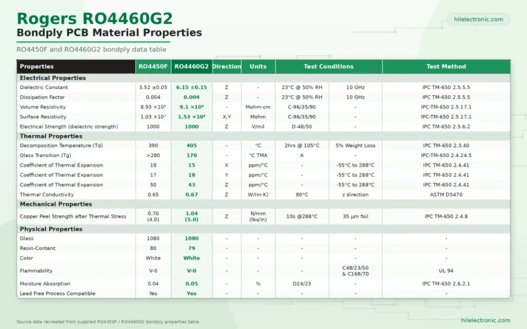
Rogers RO4460G2 Bondply PCB for High-Dk Multilayer RF Stackups
RO4460G2 bondply PCB manufacturing is a high-Dk multilayer...
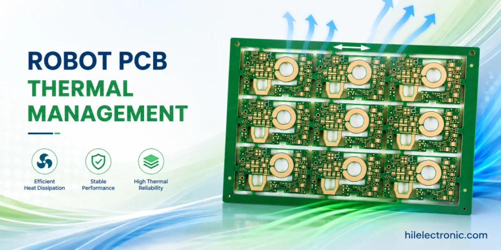
Robot PCB Thermal Management for Motors, Power Rails and Compute
Robot PCB thermal management affects service life, field...
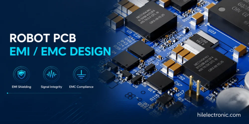
Robot PCB EMI/EMC Design for Reliable Robotics
Robot PCB EMI and EMC design affects whether a robot can...
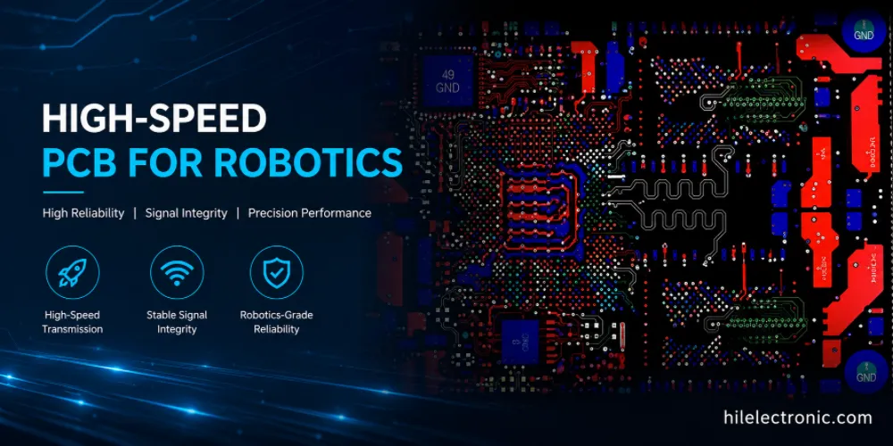
High-Speed PCB for Robotics: PCIe, DDR, MIPI and Ethernet Layout
High-speed PCB manufacturing for robotics supports data...
How to get a quote for PCBs
Let‘s run DFM/DFA analysis for you and get back to you with a report. You can upload your files securely through our website. We require the following information in order to give you a quote:
-
- Gerber, ODB++, or .pcb, spec.
- BOM list if you require assembly
- Quantity
- Turn time
In addition to PCB manufacturing, we offer a comprehensive range of electronic services, including PCB design, PCBA, and turnkey solutions. Whether you need help with prototyping, design verification, component sourcing, or mass production, we provide end-to-end support to ensure your project’s success.
For PCBA services, please provide your BOM (Bill of Materials) and any specific assembly instructions. We also offer DFM/DFA analysis to optimize your designs for manufacturability and assembly, ensuring a smooth production process.