
Material Selection for Copper Coin PCBs: Thermal Conductivity & Reliability

Copper coin PCBs serve critical roles in high-power modules, test boards, and thermal management applications where efficient heat dissipation is paramount. The selection of copper coin material directly determines both thermal conductivity performance and long-term interface reliability.
As power densities increase in SiC and GaN devices, engineers must carefully evaluate copper purity, surface plating options, and interface treatments to ensure optimal thermal pathways. This analysis examines how material properties, electroplating specifications, and surface preparation methods influence performance and operational lifespan in demanding thermal environments.
Understanding Copper Coin Materials
Copper coins function as dedicated thermal vias embedded within PCB stackups, creating low-resistance heat flow paths from heat-generating components to heat sinks or thermal planes. Unlike standard through-hole vias, these solid copper cylinders offer significantly higher thermal mass and conductivity. The copper coin material composition fundamentally determines heat transfer efficiency, with thermal conductivity ranging from 380 to 398 W/m·K depending on purity grades and manufacturing processes.
Common Copper Types
- ETP (Electrolytic Tough Pitch) copper contains approximately 0.04% oxygen and represents the most cost-effective option for moderate thermal applications. Its thermal conductivity typically reaches 380-385 W/m·K with good mechanical strength.
- OFC (Oxygen-Free Copper) eliminates oxygen content to below 0.001%, achieving thermal conductivity up to 398 W/m·K while offering superior ductility and resistance to hydrogen embrittlement.
High-power applications requiring maximum thermal performance typically specify OFC grades despite the 15-25% cost premium over ETP materials.
Performance Comparison
| Property | ETP Copper | OFC Copper |
|---|---|---|
| Thermal Conductivity | 380-385 W/m·K | 395-398 W/m·K |
| Oxygen Content | ~0.04% | <0.001% |
| Ductility | Good | Excellent |
| Cost | Lower (baseline) | 15-25% premium |
| Best Applications | General thermal management | High-power SiC/GaN modules |
Influence of Copper Purity on Thermal Conductivity and Reliability
Purity and Thermal Performance
Higher copper purity enhances phonon-mediated thermal conductivity by increasing the electron mean free path. OFC copper (≥99.99% purity) achieves peak thermal performance, while gains above 99.95% are minimal, making ultra-pure grades often economically inefficient. Impurities such as oxygen, sulfur, and iron introduce lattice defects that scatter heat, reducing conductivity by 3–5% compared to oxygen-free copper.
Mechanical Trade-offs at Elevated Temperatures
Pure copper softens above 150°C, potentially compromising structural integrity under mechanical stress or vibration. Engineers must balance maximum thermal conductivity with mechanical strength, sometimes using minor alloying or optimized coin geometry to maintain support without significantly impacting heat transfer.
Thermal Cycling Fatigue Resistance
Copper purity strongly affects thermal cycling durability. OFC copper exhibits superior resistance to fatigue crack initiation due to enhanced ductility and reduced grain boundary oxidation. Test data show OFC specimens survive 2,000–3,000 cycles between -40°C and 150°C, compared to 1,500–2,000 cycles for ETP copper, making OFC preferable in automotive and aerospace applications where thermal cycling drives failure.

Copper Coin PCBs
Surface Plating and Interface Treatment
Role of Electroplating in Copper Coin Assemblies
Surface plating in copper coin PCBs serves three key purposes: preventing oxidation, enhancing solder wettability, and controlling interface thermal resistance. Each layer adds some thermal impedance, so plating selection must balance long-term reliability with minimal thermal resistance. Proper electroplating directly affects both assembly yield and operational thermal stability.
Common Plating Systems Comparison
- ENIG (Electroless Nickel Immersion Gold) – Excellent oxidation resistance and shelf life (>12 months), suitable for standard reliability applications; nickel layer adds 10–15 mm²·K/W thermal resistance.
- Silver Plating – High thermal conductivity near bulk copper, low contact resistance; ideal for high-frequency or maximum heat transfer applications.
- Tin Plating – Economical but oxidizes quickly; best for cost-sensitive applications with controlled environments and shorter lifetimes.
Plating Thickness and Thermal Resistance Balance
Plating thickness affects thermal interface resistance:
-
Thicker nickel improves oxidation protection but increases thermal impedance.
-
Optimal ENIG: 3–5 μm Ni + 0.05–0.1 μm Au, balancing protection and heat transfer.
-
Silver plating: 2–4 μm achieves similar protection with minimal thermal penalty.
-
Diffusion barrier layers prevent copper migration into solder joints during thermal aging, critical for continuous operation above 125°C.
Interface Reliability: Bonding and Oxidation Control
Interface Bonding as a Critical Success Factor
The copper coin–substrate interface is the primary potential failure point in thermal management systems. Reliable bonding is essential for minimizing thermal resistance and ensuring mechanical integrity.
- FR4 substrates: Prepreg adhesion combined with mechanical interlocking determines bond strength.
- IMS and ceramic substrates: Require brazing or direct bonded copper processes, demanding precise surface preparation and controlled thermal profiles during attachment.
Surface Preparation and Activation
Oxide-free copper surfaces are crucial for strong interface bonding. Effective treatments include mechanical brushing, micro-etching, or plasma cleaning to remove native oxides and contaminants.
- Optimal oxide thickness: <100 nm
- Activation creates micro-roughness to enhance mechanical interlocking.
- Timing is critical: surfaces should be assembled within 2–4 hours to prevent oxide reformation.
Solder Wetting and Void Control
Interface voids increase thermal resistance and create stress concentration points, accelerating fatigue failure.
- Maintain voids <5% of interface area.
- Achieved via controlled solder paste application, optimized reflow profiles, and vacuum reflow for critical applications.
- Wetting angle measurement: angles <30° indicate excellent wettability and minimal void risk.
Long-term Degradation Mechanisms
Thermal cycling and humidity exposure drive interface degradation:
- CTE mismatch between copper and substrate induces cyclic shear stress → delamination or crack propagation.
- Moisture ingress accelerates corrosion at the copper-solder interface, especially in non-hermetic packages.
- Validation tests: thermal cycling (-40°C to 150°C, 1000+ cycles) and 85/85 humidity (85°C, 85% RH, 1000 hours) confirm reliability for intended applications.

Copper Coin PCB Manufacturing
Material Selection Guidelines for Long-Term Reliability
Application-Specific Recommendations
Material selection for copper coin material systems requires matching thermal requirements, environmental conditions, and cost constraints to material properties:
- High-power modules (SiC/GaN): OFC copper with ENIG plating provides optimal thermal performance and long-term stability for continuous operation above 150°C
- Automotive ECUs: ETP copper with silver plating balances cost and performance for -40°C to 125°C thermal cycling environments
- Test socket PCBs: OFC copper with ENEPIG plating ensures contact reliability through thousands of insertion cycles while maintaining stable thermal characteristics
- Consumer electronics: ETP copper with tin plating provides adequate thermal performance at minimum cost for moderate duty cycles
System Integration Considerations
Successful implementation requires matching copper coin specifications to the complete thermal system. Material selection must consider substrate CTE compatibility, available assembly processes, and operating environment. High-reliability applications benefit from material systems validated through accelerated life testing.
Matching plating systems to assembly processes prevents processing issues—for example, ENIG withstands multiple reflow cycles while maintaining solderability, whereas OSP coatings degrade after second reflow. Proper material selection and process integration ensure the copper coin thermal path performs reliably throughout the product lifecycle.
Conclusion: Balancing Conductivity, Cost, and Reliability
Copper coin material selection directly influences both immediate thermal conductivity and long-term interface reliability. Choosing the right copper grade and surface treatment is essential to ensure stable performance under continuous power and thermal stress. Key takeaways:
-
Material selection defines performance – OFC copper delivers maximum thermal conductivity for high-power modules, while ETP copper provides a cost-effective balance for moderate thermal applications.
-
Surface finish impacts stability – Reliable systems require controlled plating thickness, oxidation prevention, and strong metal-to-substrate bonding.
-
Integrated approach ensures reliability – Combining high-purity copper, optimized plating, and precise interface preparation enables superior thermal management and durability.
-
Industry trend – Next-generation power and automotive electronics increasingly adopt OFC copper with advanced surface plating for improved thermal performance and mechanical stability.
As electronic designs push toward higher power density and miniaturization, integrated material and process optimization will remain the foundation of reliable copper coin PCB technology.
Highleap Electronics offers precision copper coin PCB manufacturing with material systems tailored for thermal performance and reliability. Our engineering team provides material selection support and thermal design validation for advanced applications in automotive, industrial, and power electronics markets.

Recommended Posts
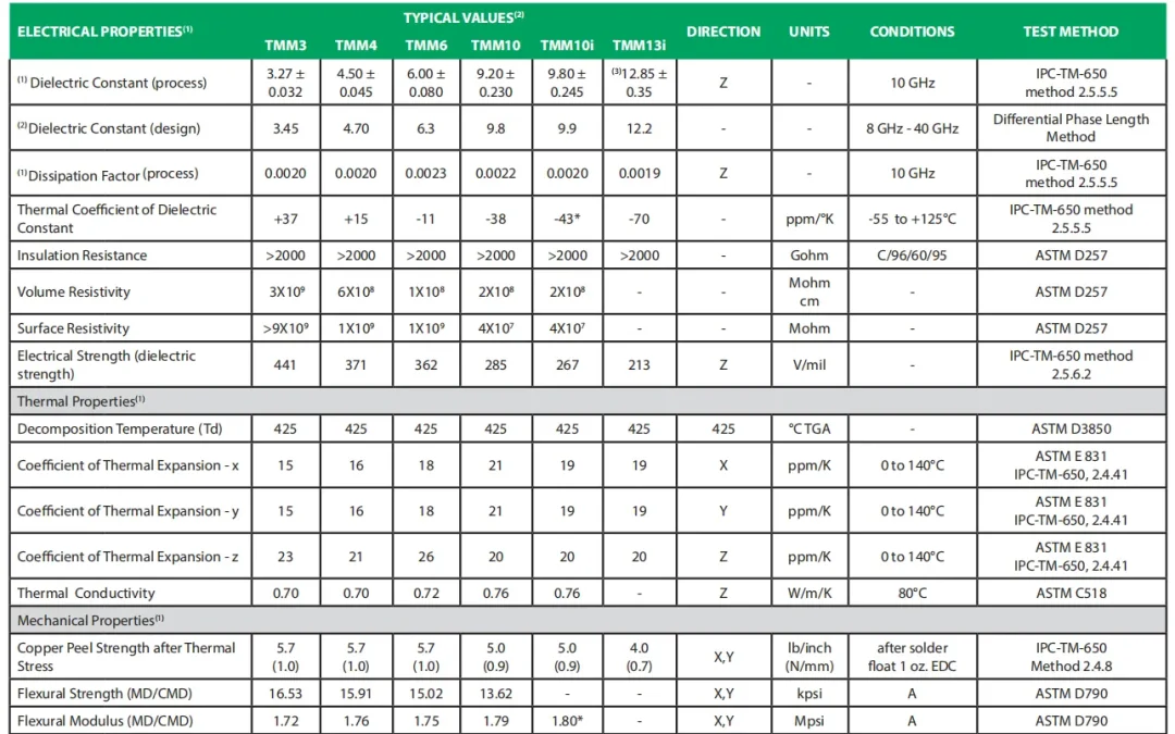
Rogers TMM High-Frequency PCB Guide
A Rogers TMM high-frequency PCB is a printed circuit board...
Glass Fiber Cloth Shortage PCB Cost and Supply
Table of contents The Role of Glass Fiber Cloth in PCB...
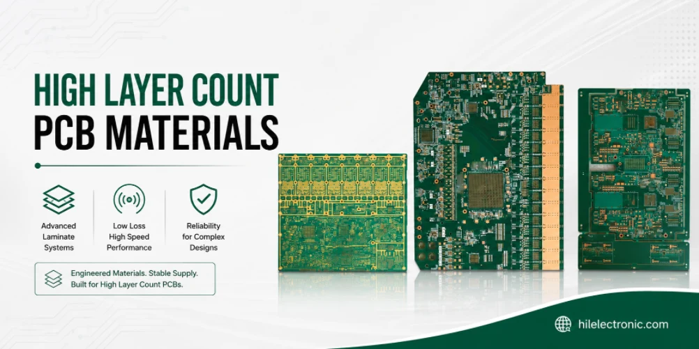
High Layer Count PCB Materials for Multilayer Boards
Table of contents Material Requirements for High Layer...
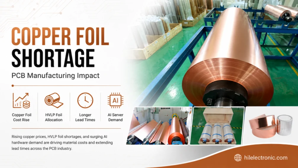
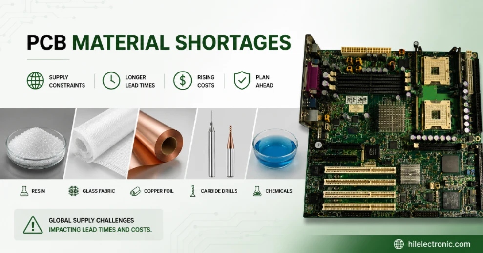
Copper Foil Shortage Impact on PCB Manufacturing
On this page Why Copper Foil Is Critical for PCB...
How to get a quote for PCBs
Let‘s run DFM/DFA analysis for you and get back to you with a report. You can upload your files securely through our website. We require the following information in order to give you a quote:
-
- Gerber, ODB++, or .pcb, spec.
- BOM list if you require assembly
- Quantity
- Turn time
In addition to PCB manufacturing, we offer a comprehensive range of electronic services, including PCB design, PCBA, and turnkey solutions. Whether you need help with prototyping, design verification, component sourcing, or mass production, we provide end-to-end support to ensure your project’s success.
For PCBA services, please provide your BOM (Bill of Materials) and any specific assembly instructions. We also offer DFM/DFA analysis to optimize your designs for manufacturability and assembly, ensuring a smooth production process.