
Copper Coin PCB Reliability Testing and Inspection

In high-power electronics, copper coin PCBs must withstand extreme thermal and mechanical stresses that would compromise conventional board designs. These specialized circuit boards embed thick copper coins directly into cavity structures to enhance thermal dissipation in power semiconductor applications.
The copper coin PCB reliability test has become an essential validation process for manufacturers targeting automotive power modules, industrial inverters, and high-current switching applications. Without rigorous testing, hidden defects such as interfacial voids or inadequate bonding can lead to premature field failures under thermal cycling conditions.
Why Copper Coin PCB Reliability Test is Critical
The copper coin structure differs fundamentally from standard copper foil lamination. Instead of continuous copper layers, thick copper discs are mechanically embedded into milled cavities and bonded with resin systems. This localized metal insertion creates multiple material interfaces where coefficient of thermal expansion mismatches and bonding quality directly affect long-term performance.
Common Failure Mechanisms in Copper Coin PCBs
Four primary failure modes threaten copper coin PCB reliability:
- Interfacial voids – Air pockets between resin and copper reduce thermal contact area and create stress concentration points
- Coin lift-off – Insufficient bonding strength causes separation under thermal expansion forces
- Resin cracking – Incomplete cavity fill or incompatible cure profiles generate cracks during reflow
- Surface oxidation – Contaminated bonding interfaces compromise adhesion strength and thermal conductivity

Copper Coin PCBs
Key Inspection Procedures in Copper Coin PCB Fabrication
Production-stage inspection identifies structural defects before boards enter reliability testing or customer qualification. Systematic quality checks at critical fabrication steps prevent defective units from advancing through manufacturing.
This page is specific to copper coin thermal structures and their reliability checks. For a general board test overview, use circuit board testing guide; for bare-board continuity, isolation, and fixture planning, see PCB electrical testing.
Dimensional Inspection
Cavity depth measurement ensures adequate space for coin embedding without excessive resin thickness above the copper surface. Coin diameter and thickness must conform to design tolerances to maintain proper fit within milled cavities. Surface planarity across the embedded region affects subsequent lamination quality and copper thickness uniformity.
Surface Cleanliness Check
Copper coin surfaces undergo chemical cleaning and micro-roughening to promote resin adhesion. Inspection protocols verify complete oxide removal and appropriate surface roughness levels before embedding. Any remaining contamination or excessive oxidation creates weak bonding interfaces that fail during thermal stress.
X-ray Inspection
Non-destructive X-ray analysis reveals internal voids between embedded coins and surrounding resin without physical sectioning. This technique also verifies coin alignment accuracy within cavities and detects incomplete resin filling in high-aspect-ratio structures. Advanced X-ray computed tomography provides three-dimensional void mapping for critical applications.
Cross-Section Microsection Analysis
Destructive cross-sectioning through embedded coin regions exposes the actual bonding layer thickness and resin fill quality. Microscopic examination reveals interfacial defects, resin penetration into surface roughness features, and any separation at critical interfaces. This analysis serves as the definitive verification method for bonding quality assessment.
Visual and AOI Inspection
Automated optical inspection systems verify solder mask alignment over embedded regions and detect surface irregularities that might indicate subsurface defects. Visual examination confirms proper coin embedding depth and identifies any mechanical damage to cavity edges or exposed copper surfaces.

X-ray inspection
Copper Coin PCB Reliability Test Methods
Reliability testing validates that copper coin PCBs maintain performance under thermal and mechanical stress conditions representative of actual operating environments. These tests accelerate failure mechanisms to predict field performance and verify design margins.
Thermal Cycling Test
Following IPC-9701 protocols, copper coin PCB reliability test specimens undergo repeated temperature excursions between -40°C and 125°C for one thousand cycles minimum. This thermal fatigue test stresses the embedded coin interfaces and solder joints simultaneously. Contact resistance measurements before and after cycling quantify interface degradation, while cross-sectional analysis after testing reveals any interfacial separation or crack propagation.
Peel Strength Test
Mechanical peel testing measures bonding force required to separate embedded copper coins from surrounding substrate material. Test results are compared against standard copper foil peel strength values to verify adequate adhesion. Reduced peel strength indicates insufficient surface preparation, incomplete resin cure, or contamination at bonding interfaces.
Cross-Section and SEM Analysis
Scanning electron microscopy examination of polished cross-sections provides high-resolution imaging of resin-copper interfaces and reveals microscopic defects invisible to optical inspection. This analysis identifies incomplete resin penetration into surface roughness, interfacial void populations, and any intermetallic compound formation at bonding layers.
Thermal Shock and Power Cycling Test
Rapid temperature transitions between extreme hot and cold conditions simulate actual power-on and power-off events in operational equipment. Power cycling tests apply electrical current through copper coin structures while monitoring temperature rise and thermal resistance changes. These tests validate thermomechanical compatibility between embedded copper and substrate materials under realistic load profiles.

Copper Coin PCB Cross Section
IPC Standards for Copper Coin PCB Reliability Test
Industry standards provide objective acceptance criteria for copper coin PCB reliability test programs. IPC-6012 establishes performance requirements for rigid printed boards including dimensional tolerances, conductor spacing, and structural integrity specifications. IPC-9701 defines reliability testing protocols specifically for solder joint performance under thermal cycling conditions.
Qualification Requirements
For copper coin PCBs used in power modules, compliance with IPC-6012 Class 3 and IPC-9701 ensures the required thermal and mechanical endurance. Key qualification criteria include:
- Thermal cycling duration – Minimum 1000 cycles across specified temperature range without measurable resistance increase
- Peel strength threshold – Bonding force must exceed 1.0 N/mm for embedded copper regions
- Visual acceptance – Zero interfacial voids or cracks visible in cross-section analysis
- Dimensional stability – Warpage must remain below 0.75% after thermal exposure per IPC-6012 Class 3
Reliability Validation and Continuous Improvement
Comprehensive copper coin PCB reliability test programs incorporate statistical analysis and failure analysis feedback loops to optimize design and manufacturing processes. Each failure mode identified during qualification testing informs corrective actions in cavity preparation, resin selection, or bonding process parameters.
Experienced manufacturers conduct regular cross-section and bonding tests to maintain stable copper coin embedding quality across production batches. Periodic verification testing on production samples ensures process consistency and detects any drift in critical parameters before customer shipments. Advanced manufacturers implement design of experiments methodologies to optimize embedding processes based on quantitative reliability data.
Conclusion
The copper coin PCB reliability test validates both immediate manufacturing quality and long-term operational durability under thermal stress. Systematic inspection protocols combined with comprehensive environmental testing provide confidence that embedded copper structures will perform reliably throughout their operational lifetime in demanding power electronics applications.
Highleap Electronics Copper Coin PCB Capabilities
- Advanced inspection systems – X-ray computed tomography and automated cross-section analysis for complete quality verification
- IPC-compliant testing – Full thermal cycling, peel strength, and power cycling test capabilities per IPC-6012 Class 3 and IPC-9701 standards
- Process optimization – Statistical process control and continuous improvement programs ensure consistent embedding quality
- Engineering support – Dedicated reliability engineering team assists with test protocol development and failure analysis
Contact our engineering team to discuss copper coin PCB reliability test requirements and qualification protocols for your specific power module design. Highleap Electronics delivers validated thermal management solutions backed by comprehensive reliability data.

Recommended Posts
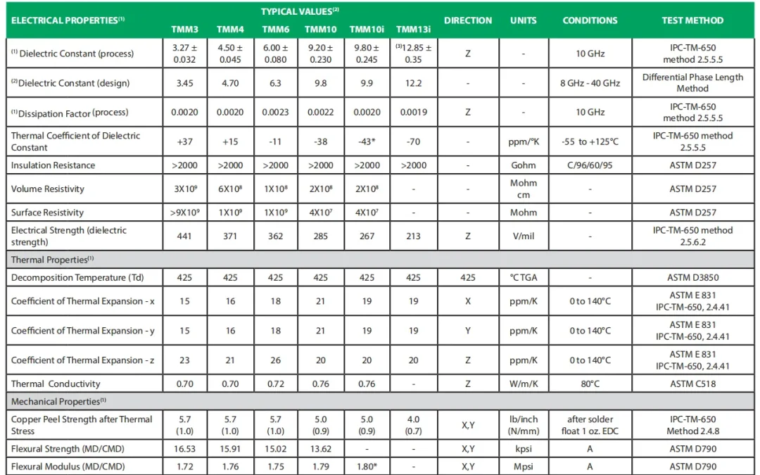
Rogers TMM High-Frequency PCB Guide
A Rogers TMM high-frequency PCB is a printed circuit board...
Glass Fiber Cloth Shortage PCB Cost and Supply
Table of contents The Role of Glass Fiber Cloth in PCB...
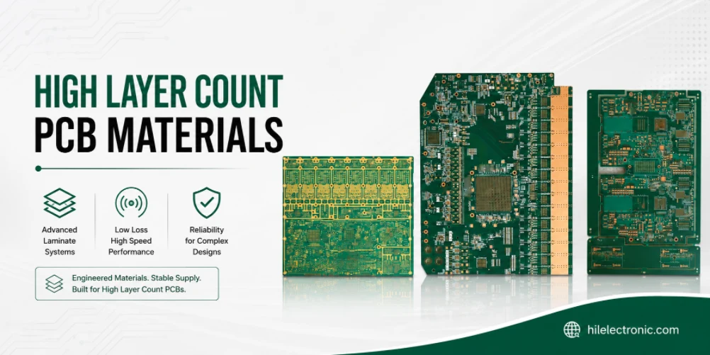
High Layer Count PCB Materials for Multilayer Boards
Table of contents Material Requirements for High Layer...
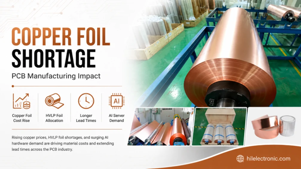
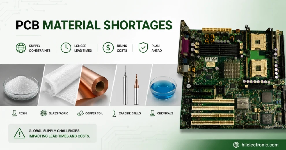
Copper Foil Shortage Impact on PCB Manufacturing
On this page Why Copper Foil Is Critical for PCB...
How to get a quote for PCBs
Let‘s run DFM/DFA analysis for you and get back to you with a report. You can upload your files securely through our website. We require the following information in order to give you a quote:
-
- Gerber, ODB++, or .pcb, spec.
- BOM list if you require assembly
- Quantity
- Turn time
In addition to PCB manufacturing, we offer a comprehensive range of electronic services, including PCB design, PCBA, and turnkey solutions. Whether you need help with prototyping, design verification, component sourcing, or mass production, we provide end-to-end support to ensure your project’s success.
For PCBA services, please provide your BOM (Bill of Materials) and any specific assembly instructions. We also offer DFM/DFA analysis to optimize your designs for manufacturability and assembly, ensuring a smooth production process.