
High Voltage Circuit Board Design and Manufacturing

Designing a high voltage circuit board (HVPCB) requires precise engineering to ensure safety, reliability, and functionality. These boards are exposed to high electric fields, posing risks such as arcing, dielectric breakdown, and component failure. Therefore, careful consideration of materials, layout, and design standards is essential. This article provides an in-depth understanding of the critical aspects of HVPCB design, including material selection, layout techniques, and safety considerations for various applications.
What Is a High Voltage Circuit Board?
A high voltage circuit board handles voltages significantly higher than those in standard electronics, often exceeding 1000V. This necessitates specific design features to maintain performance and ensure safety. Overvoltage conditions can lead to issues such as:
- Dielectric breakdown: The insulating materials fail, resulting in unintended current paths.
- Arcing: An unwanted discharge of electricity through air gaps or surface contamination.
- Thermal runaway: Excess heat generation can damage components and compromise the entire system.
Proper design ensures that these risks are mitigated while maintaining the board’s durability and longevity, even in harsh environments.
Key Materials for High Voltage Circuit Boards
1. Base Laminate Material
The base material provides insulation between copper layers and affects the board’s mechanical properties. Commonly used laminates include:
FR4:
-
- Advantages: Affordable, easy to manufacture, and provides moderate dielectric properties.
- Disadvantages: Vulnerable to contamination over time, which may reduce its reliability in high-voltage applications.
BT Epoxy:
-
- Advantages: Offers excellent resistance to heat and moisture, with robust sidewall integrity.
- Limitations: Higher cost, used primarily for specialized applications.
Polyimide and Teflon:
-
- Advantages: High dielectric strength, ideal for aerospace, military, and medical equipment.
- Limitations: High manufacturing cost and complexity.
These high-performance laminates are preferred in environments requiring extreme reliability.
2. Copper Weight
The thickness of copper in a circuit board is crucial for handling high currents. High voltage circuit boards often require heavy or extreme copper layers to prevent trace burnout:
- Heavy copper (4-10 oz): Suitable for most high-voltage applications.
- Extreme copper (10-50 oz): Necessary for power-intensive applications like particle colliders or industrial power supplies.
Thicker copper enhances both mechanical strength and heat dissipation, ensuring reliability under high-voltage stress.
3. Glass and Resin Content
The balance between glass fibers and resin affects a circuit board’s dielectric strength. High resin content with fine glass weaves improves insulation, reducing the chance of surface arcing. This is essential for applications operating under vacuum or high pressure, where air gaps can compromise insulation.
4. Comparative Tracking Index (CTI)
CTI measures the resistance of materials to electrical tracking under high voltage. Materials are rated across six CTI categories:
- Category 0: CTI > 600V (Excellent insulation properties).
- Category 1-2: CTI between 400-600V (Good for most high-voltage applications).
Using materials with higher CTI ratings ensures better performance, especially in humid or contaminated environments.
Design Techniques for High Voltage Circuit Boards
1. Creepage and Clearance Requirements
Creepage and clearance are critical spacing parameters in HVPCB design:
- Clearance: The shortest path through the air between two conductive elements.
- Creepage: The shortest distance along the board surface between two conductors.
Why These Spacings Matter?
In high-voltage applications, insufficient clearance can result in arcing through the air, while inadequate creepage may lead to surface tracking and short circuits. Environmental factors such as humidity and dust further reduce creepage insulation, making correct design even more critical.
Recommended Distances Based on Voltage (from IPC-2221):
- 0-150V: 1.0mm clearance, 1.6mm creepage
- 150-300V: 1.5mm clearance, 2.5mm creepage
- Above 1000V: Clearance and creepage may need to exceed 10-20mm, depending on environmental conditions.
2. Optimizing Trace Design
Sharp bends and corners in circuit traces can create localized electric field concentrations, increasing the chance of arcing. To avoid this:
- Use curved traces or 45-degree angles instead of 90-degree bends.
- Implement teardrop pads to reduce stress at via connections.
- Use wide traces to distribute heat and current more evenly, minimizing thermal stress.
3. Surface Finish Considerations
- ENIG (Electroless Nickel Immersion Gold): Provides a smooth surface, minimizing arcing risks.
- HASL (Hot Air Solder Leveling): May introduce surface roughness, which can encourage arcing under high voltage.
A smooth surface ensures that arcs do not form on unintended parts of the circuit board, maintaining the board’s integrity.
Manufacturing Considerations for High Voltage Circuit Boards
1. Routing and Edge Cleanup
Proper routing and edge finishing are essential in the manufacturing of high voltage circuit boards (HVPCBs). Sharp edges, burrs, or rough surfaces can create areas where arcing or electric field concentration may occur, leading to electrical failures. To address this, manufacturers use plasma cleaning or chemical treatments to remove contaminants and smooth rough edges. Plasma cleaning not only eliminates residual debris but also enhances surface adhesion for coatings, while chemical etching reduces weak points that might trigger insulation breakdown. A smooth edge finish ensures the board remains durable and resistant to electrical discharge over time.
This page remains the broad high-voltage circuit board manufacturing guide. For layout strategy and spacing decisions, use high voltage PCB design strategies; for metal-core high-voltage boards, compare the requirement with high voltage MCPCB creepage distance.
2. Conformal Coating
Applying a conformal coating provides essential protection to the circuit board against moisture, dust, and other environmental contaminants. In high voltage applications, these coatings play an additional role by preventing surface tracking—an unintended electrical path along the board’s surface. Various coatings are available based on the application: silicone is ideal for high-temperature environments, acrylic offers excellent moisture resistance, and parylene provides superior dielectric strength but is more expensive. Coatings can be applied using spray, dip, or selective methods, ensuring uniform coverage to prevent weak points where insulation could fail.
3. High Voltage Testing
Testing is a crucial part of the HVPCB manufacturing process to ensure that the board can handle extreme voltages safely. Hi-Pot testing (High Potential testing) applies a voltage higher than the operating level between conductive elements to verify that the insulation does not break down or allow leakage current. Partial discharge testing detects micro-arcs or weak points within the PCB, which can degrade the insulation over time. Both tests are essential to validate the board’s reliability under high voltage conditions, identifying and eliminating defective boards before deployment.
4. Thermal Management and Layer Alignment
In high voltage circuit boards, thermal management is critical, especially when thick copper layers are used to carry heavy currents. Manufacturers integrate thermal vias, heat sinks, or copper planes to dissipate heat efficiently and prevent thermal stress from damaging the board. Additionally, ensuring accurate layer alignment in multi-layer boards prevents layer-to-layer shorts, maintaining proper creepage and clearance distances. Precise manufacturing practices ensure that the circuit board not only withstands high voltage stresses but also remains operational over extended periods in demanding environments.
For production planning, it also helps to compare this topic with PCB design review and surface finish comparison before finalizing the fabrication or assembly package.

Compliance and Safety Standards for High Voltage Circuit Boards
High voltage circuit boards (HVPCBs) must adhere to specific design and safety standards to ensure their reliability and safe operation. One of the most critical standards is IPC-2221, which outlines design principles for creepage and clearance distances. These guidelines specify the minimum air gap (clearance) and surface distance (creepage) required between conductive elements based on the applied voltage and environmental factors such as humidity or pollution. Following IPC-2221 ensures that the board can withstand arcing and insulation failures, even in challenging operating conditions, helping prevent electrical malfunctions.
The IEC-60950-1 standard addresses safety requirements for electrical equipment, including recommendations for insulation materials used in HVPCBs. It emphasizes testing the dielectric breakdown strength of insulating components under voltage stress, ensuring they remain effective throughout the product’s life cycle. Additionally, this standard highlights the importance of evaluating operating temperatures and fault scenarios, ensuring that even in case of failure, the system does not pose safety hazards to users. Compliance with IEC-60950-1 is especially critical for industrial and information technology applications, where high voltage systems are common.
UL certification, particularly UL 796, provides independent testing to ensure that high voltage circuit boards meet consumer and industrial safety requirements. Boards must pass flammability tests (e.g., UL 94 V-0), demonstrate sufficient dielectric strength under voltage surges, and maintain their performance in high-temperature environments. Additionally, UL-certified boards are marked for traceability, ensuring that every component meets regulatory standards. UL certification helps products gain market approval and minimizes liability risks, offering manufacturers a competitive advantage.
Compliance with IPC-2221, IEC-60950-1, and UL standards ensures that HVPCBs meet global safety expectations. These standards not only protect users from electrical hazards but also ensure that boards function reliably in high-risk environments such as aerospace, medical devices, and industrial machinery. By following these regulations, manufacturers improve product safety and reliability, reduce legal liabilities, and ensure their products meet the requirements for regulated markets.
Conclusion
Designing a high voltage circuit board requires careful attention to material selection, layout design, and manufacturing techniques to ensure safety and reliability. By choosing the right laminate materials, copper thickness, and surface finishes, engineers can mitigate risks like arcing and dielectric breakdown. Adhering to creepage and clearance standards is essential for safe operation in demanding environments, from aerospace to medical equipment.
At Highleap Electronic, we specialize in PCB manufacturing and assembly, offering one-stop electronic manufacturing services tailored to your high voltage circuit board needs. Our expertise in selecting premium materials and employing advanced manufacturing techniques ensures your designs meet the highest safety and performance standards.
With these best practices in place, high voltage circuit boards can drive the cutting-edge technologies of tomorrow, enabling breakthroughs in science, medicine, and engineering. By partnering with us, you can ensure that your designs not only perform optimally but also protect users and equipment from the inherent dangers of high voltage systems. Let us help you bring your innovative projects to life with precision and reliability.
Get a Free PCB & PCBA Quote

Recommended Posts
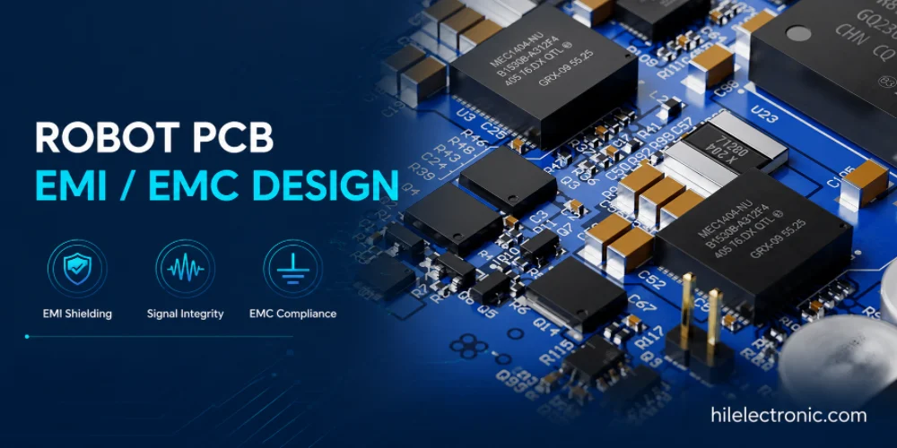
Robot PCB EMI/EMC Design for Reliable Robotics
Robot PCB EMI and EMC design affects whether a robot can...
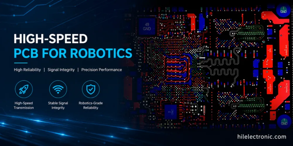
High-Speed PCB for Robotics: PCIe, DDR, MIPI and Ethernet Layout
High-speed PCB manufacturing for robotics supports data...
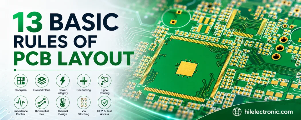
13 Basic Rules of PCB Layout (and the Failures They Prevent)
Figure 1. 13 Basic Rules Of Pcb Layout reference image for...

PCB Current Calculator: Sizing Trace Width and Vias with the IPC-2221 Formula
Figure 1. Pcb Current Calculator reference image for PCB...
How to get a quote for PCBs
Let us run DFM/DFA analysis for you and get back to you with a report.
You can upload your files securely through our website.
We require the following information in order to give you a quote:
-
- Gerber, ODB++, or .pcb, spec.
- BOM list if you require assembly
- Quantity
- Turn time
In addition to PCB manufacturing, we offer a comprehensive range of electronic services, including PCB design, PCBA (Printed Circuit Board Assembly), and turnkey solutions. Whether you need help with prototyping, design verification, component sourcing, or mass production, we provide end-to-end support to ensure your project’s success. For PCBA services, please provide your BOM (Bill of Materials) and any specific assembly instructions. We also offer DFM/DFA analysis to optimize your designs for manufacturability and assembly, ensuring a smooth production process.