
The Comprehensive Guide to IC Substrate PCBs

The evolution of electronics has been marked by a rapid increase in the miniaturization and complexity of integrated circuits (ICs). A critical component enabling this transformation is the IC substrate PCB, which has become indispensable in packaging advanced ICs, such as Ball Grid Arrays (BGA), Chip Scale Packages (CSP), and Flip Chips (FC). IC substrate PCBs serve as a fundamental platform for modern electronics, playing a central role in telecommunications, consumer electronics, aerospace, automotive, medical devices, and various other industries. This article provides a comprehensive look into the IC substrate PCB, including its functions, structure, manufacturing processes, types, applications, and how it addresses key challenges faced by customers in the industry.
What Is an IC Substrate PCB?
An IC substrate PCB is a specialized type of Printed Circuit Board (PCB) designed to house and support microchips. It serves as the platform for packaging ICs and ensuring their connection to larger electronic systems such as motherboards or circuit boards. The IC substrate PCB is a crucial component that bridges the intricate, small-scale connections of the chip and the larger-scale circuitry of the PCB.
The primary functions of an IC substrate PCB are as follows:
-
Chip Packaging: It encapsulates the bare IC chip, offering physical protection and mechanical support.
-
Routing: It establishes electrical routing between the chip and the larger circuit board, ensuring proper communication and signal transmission.
-
Thermal Management: It dissipates heat generated by the chip, helping maintain optimal operating temperatures for the IC.
-
Reinforcement and Protection: The substrate provides mechanical reinforcement to prevent damage to the delicate chip components.
In essence, the IC substrate PCB is a vital component of modern electronic systems, enabling the integration of powerful microchips into compact, high-performance devices.
IC Substrate PCB: Key Features and Characteristics
IC substrate PCBs are characterized by specific attributes that make them distinct from regular PCBs. These features are crucial for ensuring the IC substrate PCB can support advanced ICs and meet the performance requirements of modern electronics:
-
Compact Size: Typically small in dimensions, designed to accommodate a single chip or a few chips, which is essential for devices with limited space.
-
Thin Profile: Ranging from 0.1 mm to 1.5 mm in thickness, IC substrate PCBs have a thin profile, making them suitable for compact electronic devices.
-
High-Density Interconnections: With minute, laser-drilled vias and fine traces, IC substrate PCBs handle complex and high-density connections, which are necessary for integrating powerful chips.
-
Thermal Management: The substrate is designed with materials that effectively dissipate heat, ensuring that the chip remains cool and performs optimally.
-
Electrical and Mechanical Support: The substrate ensures that electrical signals are routed efficiently while also providing the mechanical strength needed to protect the IC from physical damage.
-
Customizability: With advances in manufacturing, IC substrate PCBs can be customized to suit specific needs, whether it’s for high-performance, flexible, or miniature applications.
These features ensure that IC substrate PCBs are an ideal solution for incorporating microchips into modern electronic systems. Whether used in consumer electronics, telecommunications, automotive, or aerospace, these characteristics enable IC substrate PCBs to provide reliability and efficiency across various industries.
Types of IC Substrate PCBs
IC substrate PCBs can be classified into various types based on their packaging methods, materials, and bonding technologies. Each type is suited for specific applications and offers unique advantages in terms of size, performance, and manufacturing complexity.
1. By Packaging Method
-
Ball Grid Array (BGA) IC Substrate PCB: BGA **IC substrate PCBs** use a grid of solder balls to connect the chip to the motherboard. They are known for their excellent thermal dissipation properties and ability to handle high pin counts.
-
Chip Scale Package (CSP) IC Substrate PCB: CSP **IC substrate PCBs** are designed for compact, low-pin-count ICs that are roughly the same size as the chip itself.
-
Flip Chip (FC) IC Substrate PCB: Flip chip **IC substrate PCBs** involve flipping the chip over and connecting it to the substrate using solder bumps, minimizing signal loss and interference.
-
Multi-Chip Module (MCM) IC Substrate PCB: MCM **IC substrate PCBs** integrate multiple chips with different functions into a single package, ideal for space-saving and miniaturization.
2. By Material Type
-
Rigid IC Substrate PCB: Made from materials such as epoxy resin or ABF resin, these are widely used in electronic applications due to their mechanical stability.
-
Flexible IC Substrate PCB: Flexible **IC substrate PCBs** are designed to be bendable, making them ideal for flexible electronics and wearables.
-
Ceramic IC Substrate PCB: Ceramic **IC substrate PCBs** offer excellent thermal conductivity and stability at high temperatures, suitable for power electronics and RF circuits.
3. By Bonding Technology
-
Wire Bonding: Involves connecting the chip to the substrate using fine wires, commonly used for low- to medium-pin count ICs.
-
Tape Automated Bonding (TAB): The chip is attached to a flexible substrate using pressure-sensitive adhesive, commonly used for thin and flexible designs.
-
Flip Chip Bonding: Flip chip bonding offers low signal interference and excellent thermal dissipation, ideal for high-performance applications.

IC Substrate Manufacturing Challenges
The manufacturing of IC substrates is complex, as it involves various technical challenges that must be addressed to ensure high performance, reliability, and precision.
1. Material Handling and Thickness Control
IC substrates are often thin, especially when the board is less than 0.2 mm thick. This makes them prone to warping and deformation during manufacturing. To overcome this challenge, manufacturers must use advanced lamination techniques, precise layer positioning, and strict control over shrinkage and warpage during the fabrication process.
2. Microvia and Fine Line Technology
The need for high-density interconnects requires the use of microvia technology, which involves laser drilling tiny holes to connect different layers of the substrate. The challenge lies in ensuring uniform via diameters and filling the vias with copper without defects. Additionally, fine line technology is crucial for creating narrow conductive traces that can support high-frequency signals.
3. Patterning and Copper Plating
Copper plating and patterning are essential for defining the circuit design on the substrate. This requires precise control over the plating thickness, as well as techniques like photolithography to ensure that the traces are accurately formed without defects.
4. Surface Finish and Solder Mask Application
The surface finish of the IC substrate plays a vital role in its performance. The surface must be smooth, with a uniform finish, to ensure reliable electrical connections and reduce the risk of oxidation. The application of the solder mask must also be precise to avoid defects that could impact the substrate’s performance.
How We Address Industry-Specific Needs
We recognize that different industries require specialized solutions to meet their unique technical demands. Our IC substrates are engineered to overcome the specific challenges faced in diverse sectors. Below, we detail how our solutions address the critical requirements for high-performance, reliability, and precision.
Advanced Thermal Management for High-Performance Applications
In modern electronics, particularly high-performance devices, thermal management is an ever-growing concern. As semiconductor devices become smaller and more powerful, the challenge of managing heat dissipation increases significantly, as overheating can lead to thermal failure and reduced component lifespan.
Solution: To address these thermal challenges, we utilize advanced materials such as ceramic-based substrates (e.g., aluminum oxide and aluminum nitride) and metal-coated polymers. These materials provide exceptional thermal conductivity, allowing for efficient heat dissipation from high-power ICs. Additionally, our designs incorporate via-array cooling structures and thermally conductive die attach adhesives, which ensure that heat is effectively managed across the substrate. These innovations help ensure that electronic devices operate within optimal temperature ranges, even in demanding environments like automotive, telecommunications, and industrial applications.
Customization for Specialized Packaging Requirements
Different industries demand substrates that can meet very specific physical, electrical, and thermal requirements. Generic off-the-shelf solutions often fail to meet these highly specialized needs, particularly in fields such as aerospace, medical devices, and defense, where precision and customization are paramount.
Solution: We offer highly customizable IC substrates that are engineered to meet the exact specifications of each application. By using tailored dielectric materials (e.g., BT resin, epoxy-based resins, or flexible polyimides), we can adjust parameters such as thermal coefficient of expansion (CTE), dielectric constant, and voltage withstand capabilities. Additionally, our substrates can be adapted for specific packaging methods, including Ball Grid Arrays (BGA), Chip Scale Packages (CSP), and Flip Chip (FC) technologies. This enables us to meet the requirements of applications ranging from high-frequency RF circuits to miniaturized wearable electronics, ensuring the substrates perform reliably in compact form factors without compromising on functionality.
Ensuring Reliability in Extreme Environments
IC substrates used in mission-critical applications such as aerospace, military, and automotive electronics must be able to endure extreme operating conditions. These include high temperatures, significant mechanical stress, exposure to vibrations, and challenging environmental conditions, such as humidity and corrosive atmospheres. Substrates must also ensure long-term electrical stability under these harsh conditions.
Solution: We specialize in high-reliability IC substrates that incorporate ceramic and high-temperature-resistant materials, ideal for applications requiring extreme robustness. Our substrates are made using materials with a low CTE to ensure mechanical stability and thermal expansion compatibility with other materials in the assembly. Advanced flip-chip bonding and solder bumping techniques ensure that the connections remain reliable even under extreme thermal cycling and mechanical stress. For example, in aerospace applications, our IC substrates can endure high-vibration environments and significant temperature fluctuations, while for automotive systems, they can withstand thermal shock and electromagnetic interference (EMI) without performance degradation.
Precision in Manufacturing for High-Density Interconnects
As the demand for miniaturization increases, substrates need to support more complex interconnects in smaller form factors. Achieving high-density interconnects (HDI) with precise microvias and fine traces is essential for advanced IC packaging solutions, particularly in consumer electronics, telecommunications, and computing.
Solution: Our substrates are engineered using laser-drilled microvias and fine-line etching techniques to ensure the creation of high-density, high-performance circuits. These microvias are filled with electroless copper to maintain signal integrity and electrical continuity. Additionally, we employ multi-layer build-up technology to achieve more complex routing and ensure that signal transmission is efficient even at high frequencies. This is crucial for applications in sectors such as 5G communication, high-performance computing, and automotive electronics, where compact designs and high-density interconnections are essential.
Our IC substrates provide solutions tailored to the specific demands of industries ranging from aerospace and defense to medical and automotive sectors. By employing cutting-edge materials, advanced manufacturing techniques, and a deep understanding of industry needs, we help our customers achieve optimal performance, reliability, and cost-effectiveness. Whether you require thermal management, customization, or durability under extreme conditions, our IC substrates are designed to meet and exceed your expectations.
Conclusion
IC substrate PCBs are a fundamental component in modern electronics, enabling the integration of advanced integrated circuits (ICs) into compact, high-performance devices. These substrates are critical for industries ranging from consumer electronics to aerospace, providing essential mechanical support, electrical routing, and thermal dissipation. As the demand for smaller, more efficient electronics grows, the role of high-quality PCB manufacturers becomes even more essential.
At Highleap Electronics, we specialize in PCB manufacturing and PCB assembly, offering cutting-edge solutions for the most complex IC substrate PCB applications. Our precision-engineered PCBs are designed to meet the most demanding standards in industries such as automotive, telecommunications, medical devices, and aerospace. By leveraging state-of-the-art technology and advanced manufacturing techniques, we provide high-performance, customized PCB solutions that ensure long-term reliability and optimal functionality.
Whether you’re looking for high-density interconnect (HDI) PCBs, flexible PCBs, or rigid PCBs, Highleap Electronics is your trusted partner in developing high-quality, cost-effective solutions that meet the specific needs of your business. Our commitment to innovation and customer satisfaction has made us a leading PCB supplier, and we are proud to be at the forefront of PCB assembly and IC substrate solutions.
With Highleap Electronics, you can count on a reliable supply chain, quick turnaround times, and top-notch customer support. We understand that every industry has unique needs, and we are ready to provide tailored PCB solutions that give your products a competitive edge. As electronics continue to evolve, we remain dedicated to offering the best PCB manufacturing and assembly services to help you stay ahead in the market.
Get a Free PCB & PCBA Quote

Recommended Posts
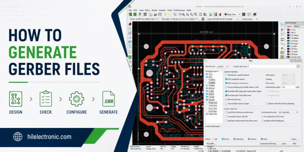
How to Generate Gerber Files for PCB Manufacturing
Figure 1. how to generate Gerber files image for Highleap...
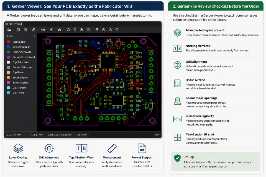
Gerber File Review Checklist: How to Check PCB Files Before You Order
Figure 1. Gerber file review catches missing layers, drill...
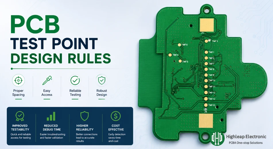
PCB Test Point Design Rules for Debug and ICT
Figure 1. PCB test point design rules help make debugging,...
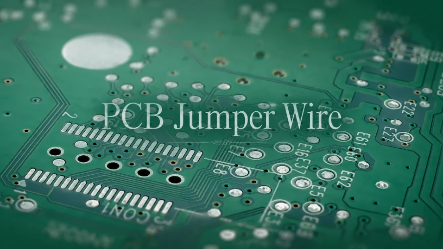
PCB Jumper Wire: Uses, Types, and Design Tips
Figure 1. PCB jumper wires are useful for prototypes and...
How to get a quote for PCBs
Let us run DFM/DFA analysis for you and get back to you with a report.
You can upload your files securely through our website.
We require the following information in order to give you a quote:
-
- Gerber, ODB++, or .pcb, spec.
- BOM list if you require assembly
- Quantity
- Turn time
In addition to PCB manufacturing, we offer a comprehensive range of electronic services, including PCB design, PCBA (Printed Circuit Board Assembly), and turnkey solutions. Whether you need help with prototyping, design verification, component sourcing, or mass production, we provide end-to-end support to ensure your project’s success. For PCBA services, please provide your BOM (Bill of Materials) and any specific assembly instructions. We also offer DFM/DFA analysis to optimize your designs for manufacturability and assembly, ensuring a smooth production process.