
The Ultimate Guide to Microwave PCB Design

Microwave PCB design is a critical field of high-frequency circuit implementation, requiring a deep understanding of electromagnetic principles and precise engineering to meet the demands of modern, complex applications. The design of microwave circuits involves several challenges not typically encountered in low-frequency PCB designs. These challenges include high-speed signal integrity, impedance control, material considerations, and manufacturing precision. Below is a detailed exploration of the primary challenges in microwave PCB design and the techniques used to address them.
1. Key Challenges in Microwave PCB Design
Microwave PCBs are typically employed in applications operating at frequencies above 1 GHz, often exceeding 30 GHz in some systems. These high-frequency signals exhibit unique characteristics that require specialized design techniques. Understanding these challenges is essential for ensuring the performance, reliability, and manufacturability of microwave PCBs.
Key Design Challenges:
-
Wave Impedance Stability: Achieving and maintaining consistent impedance across the PCB stackup is critical for high-frequency applications. A typical requirement is maintaining a characteristic impedance of 50Ω with a tolerance of ±5%, especially across multi-layer designs where impedance mismatches can lead to signal reflection and power loss.
-
Dielectric Dispersion: At high frequencies, the dielectric constant (Dk) of materials varies with frequency. For example, substrates like Rogers 4350B have a Dk of 3.48±0.05 at 10GHz, which requires careful simulation to account for the frequency-dependent behavior. This variability can result in signal delay, phase shifts, and reflections if not addressed correctly.
-
Surface Roughness Impact: The roughness of copper traces can significantly influence insertion loss and signal integrity, especially at higher frequencies. For instance, a copper roughness of 0.4μm can result in an insertion loss of 0.15 dB/inch at 40GHz. To minimize such effects, manufacturers need to control the copper surface texture and implement techniques like smooth copper plating.
-
Via Stub Resonance: Via stubs can create unwanted resonant frequencies that interfere with the signal path. A typical issue arises when via stubs resonate at frequencies such as 28GHz (λ/4 via stubs), causing 0.3dB null points in signal transmission. Back-drilling techniques are used to reduce these stubs, with tight positional accuracy of less than 50μm for best results.
2. Material Considerations in Microwave PCB Design
Material selection plays a crucial role in determining the performance of microwave PCBs. Advanced materials are required to handle the high frequencies, maintain signal integrity, and ensure efficient power transmission.
Key Material Properties:

The material’s dielectric constant (Dk), loss tangent (Df), and thermal conductivity are the primary considerations when selecting a substrate for microwave PCBs. For instance, materials with low Df values, such as Taconic RF-35, are ideal for applications that require minimal signal loss, such as automotive radar or satellite communications.
Emerging Material Technologies:
-
PTFE-Ceramic Composites: These materials offer excellent high-frequency performance, with a loss tangent as low as 0.0012 for applications like 77GHz automotive radar.
-
Liquid Crystal Polymer (LCP): With flexibility and low loss tangent (0.0025), LCP is used in high-frequency designs where both flexibility and performance are essential, such as in phased array antennas.
-
Silicon-Based Substrates: For packaging mmWave ICs, silicon substrates with Through-Silicon Via (TSV) densities greater than 10^4/cm² are used, enabling high-density, high-frequency applications like 5G systems.
3. Precision Manufacturing for Microwave PCBs
Microwave PCBs require advanced manufacturing techniques to meet the high-performance demands of frequencies exceeding 1 GHz, particularly above 30 GHz. These techniques ensure that microwave circuits maintain integrity and reliability, crucial for applications in 5G, radar, satellite communication, and defense systems.
Manufacturing Techniques for Microwave PCBs
- Laser Direct Imaging (LDI)
LDI is essential for creating fine lines and accurate features in microwave PCB designs, allowing precision as small as 5μm. This ensures consistent impedance control, which is vital for high-frequency performance, preventing signal reflections and power loss. - Plasma Etching
Plasma etching ensures cleanly etched copper traces with precise sidewall angles, maintaining controlled impedance and signal integrity, especially at higher frequencies where even minor variations can cause losses. - Surface Modification (Nitrogen Plasma Treatment)
Nitrogen plasma treatment improves adhesion and reduces insertion loss by enhancing copper-to-dielectric bonding, ensuring smoother surfaces for better signal flow and minimizing resistance. - Conformal Shielding
Conformal shielding, often with Ni/Au coatings, prevents electromagnetic interference (EMI) and enhances signal fidelity by reducing noise and preventing crosstalk, which is crucial in high-frequency designs.
Manufacturing Challenges in Microwave PCB Production
Several challenges must be managed to ensure the performance of microwave PCBs, including dimensional stability, copper roughness, and via formation.
- Dimensional Stability
Thermal expansion control is vital during the lamination process to prevent misalignment or delamination that could affect performance. Maintaining <0.3‰ expansion ensures precise signal integrity throughout the board’s lifecycle. - Copper Roughness
The roughness of copper traces impacts signal transmission. For higher frequencies, it is essential to control copper surface roughness (Rq < 1.2μm) to minimize insertion loss and preserve signal integrity. - Via Formation
Microwave PCBs require precise microvia formation, often achieved with laser drilling. Ensuring high accuracy is critical, especially for high-density interconnect designs used in applications like 5G and advanced radar systems.
Mastering these specialized techniques is crucial for ensuring the high performance of microwave PCBs in demanding applications. For more details on the materials and processes involved, explore our microwave PCB materials page. To learn more about our capabilities in precision manufacturing, visit our microwave PCB manufacturing services. For an overview of our full solutions, check out our microwave PCB page.

4. Signal Integrity and Simulation in Microwave PCB Design
Signal integrity is crucial for high-frequency circuit performance in microwave PCB design. As frequencies exceed 30GHz, traditional methods are insufficient, requiring specialized simulation tools for precise modeling.
Key Simulation Technologies
3D Full-Wave Electromagnetic Simulation
- Tool Selection: HFSS and EMPro support simulations up to 110GHz
- Core Functions: S-parameter extraction, signal path optimization, crosstalk analysis
- Performance Benefits: Early identification of signal reflection and transmission loss issues
Nonlinear Circuit Modeling
- Applications: Power amplifiers, mixers, and other nonlinear components
- Modeling Tools: ADS with X-parameter technology
- Performance Assurance: Predicts behavior under high-power conditions, avoiding signal distortion
Thermal-Electronic Co-Simulation
- Temperature Control: Ensures 64-element beamformer temperature rise < 15°C
- Simulation Software: Icepak and Flotherm thermal analysis tools
- Reliability Enhancement: Manages thermal effects in multi-layer stackups
Signal Integrity Optimization
Microwave PCB design addresses electromagnetic compatibility (EMC), insertion loss, return loss, and crosstalk. Through simulation, potential issues are predicted and resolved before manufacturing, improving design efficiency and reliability.
5. Reliability Testing and Standards in Microwave PCB Design
In microwave PCB design, ensuring long-term reliability is critical for performance in demanding environments like radar, 5G, and satellite systems. These circuits must withstand extreme temperatures, vibrations, and moisture, which can affect signal integrity. Rigorous reliability tests ensure microwave PCBs maintain performance even under harsh conditions.
Thermal Cycling
Thermal cycling tests, such as MIL-STD-883H, simulate temperature fluctuations (-55°C to +125°C) over 1000 cycles, ensuring microwave PCB materials remain stable and preventing issues like cracking or impedance shifts.
CAF Resistance
CAF resistance testing evaluates the board’s ability to withstand moisture and electrical migration under high humidity and temperature. This ensures long-term reliability in environments like automotive or aerospace applications.
HALT Testing
HALT testing exposes PCBs to 40G vibration and 150°C stress to assess durability and identify potential failure points, such as trace cracking or delamination, critical for mission-critical applications in aerospace and military systems.
Reliability testing, including thermal cycling, CAF resistance, and HALT, ensures that microwave PCBs maintain consistent performance in high-frequency applications, optimizing designs for long-term reliability.
Conclusion
Microwave PCB design requires expertise in high-frequency electronics and materials science. As demand for high-performance systems grows, engineers face challenges in impedance control, signal integrity, and precision manufacturing. With advancements in simulation, materials, and manufacturing, microwave PCBs are critical for next-generation communication systems, automotive radar, and high-frequency applications.
At Highleap Electronics, we apply our extensive PCB manufacturing and assembly expertise to meet the stringent demands of microwave designs. Our advanced manufacturing processes, including laser-direct imaging and plasma etching, ensure precision and performance for applications like radar and 5G communication devices.
Committed to quality and reliability, Highleap Electronics delivers innovative solutions and exceptional customer support, ensuring your designs perform flawlessly in real-world applications. Partner with us to elevate your microwave PCB designs.
Get a Free PCB & PCBA Quote

Recommended Posts

PCB Current Calculator: Sizing Trace Width and Vias with the IPC-2221 Formula
Figure 1. Pcb Current Calculator reference image for PCB...
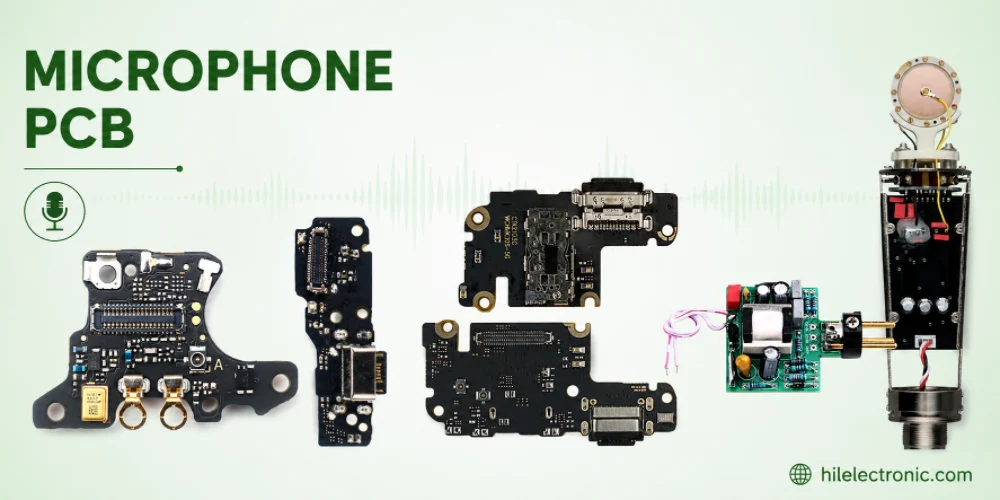
Microphone PCB Design: How the Board Itself Shapes Your Audio Quality
Figure 1. Microphone Pcb reference image for PCB...
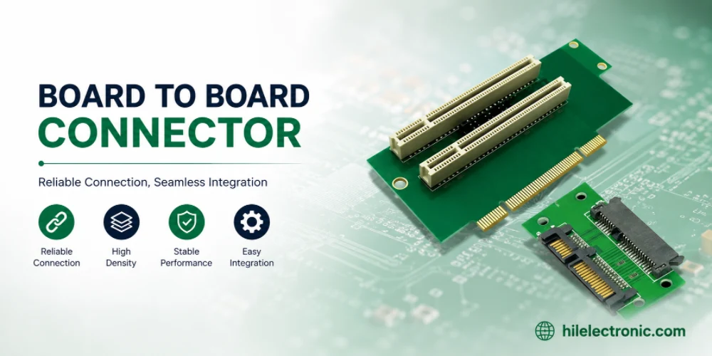
Board-to-Board Connector: Types, Specifications, and How to Select One
Figure 1. Board To Board Connector reference image for PCB...
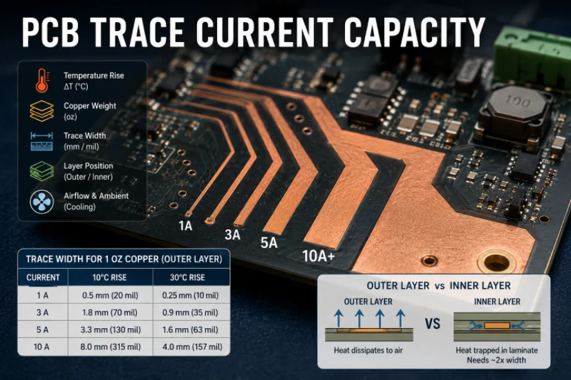
PCB Trace Width Calculator: How to Size Traces for Current, Voltage Drop, and Impedance
Figure 1. A PCB trace width calculator is a starting point...
How to get a quote for PCBs
Let us run DFM/DFA analysis for you and get back to you with a report.
You can upload your files securely through our website.
We require the following information in order to give you a quote:
-
- Gerber, ODB++, or .pcb, spec.
- BOM list if you require assembly
- Quantity
- Turn time
In addition to PCB manufacturing, we offer a comprehensive range of electronic services, including PCB design, PCBA (Printed Circuit Board Assembly), and turnkey solutions. Whether you need help with prototyping, design verification, component sourcing, or mass production, we provide end-to-end support to ensure your project’s success. For PCBA services, please provide your BOM (Bill of Materials) and any specific assembly instructions. We also offer DFM/DFA analysis to optimize your designs for manufacturability and assembly, ensuring a smooth production process.