
Nvidia PCB Solutions for Nvidia-Powered Applications

In today’s fast-evolving technology landscape, Nvidia has become a cornerstone in industries ranging from AI computing and data centers to autonomous vehicles and edge devices. As companies innovate on top of Nvidia’s GPU platforms, CUDA ecosystem, and AI development boards, they increasingly require custom PCB manufacturing and assembly services that can seamlessly integrate with Nvidia-powered solutions.
At Highleap Electronics, we specialize in developing and customizing PCBs that align perfectly with the performance, thermal, and form factor requirements of Nvidia-based applications.
Why Custom PCBs Are Critical for Nvidia-Based Hardware
Nvidia GPUs and SoCs can deliver extraordinary computational throughput, but they only reach that level consistently when the surrounding electronic design is just as disciplined. Off-the-shelf boards rarely align perfectly with high-speed layout rules, thermal budgets, or form-factor constraints. That is where a well-engineered custom PCB makes the difference—turning raw silicon potential into reliable, deployable performance.
1. High-speed signal integrity
Modern Nvidia accelerator boards push enormous data rates across PCIe, NVLink, GDDR, and high-speed SerDes lanes. Minute discontinuities—via stubs, skew, impedance drift, poorly managed reference planes—can quietly erode bandwidth or raise error rates. A custom stack-up, tuned trace geometries, length-matching discipline, and controlled impedance routing (especially across layer transitions) preserve eye diagrams and timing margins. Proven GPU server PCB manufacturing experience shortens the trial-and-error cycle here.
2. Thermal management under sustained load
AI training and inference workloads rarely run “bursty” anymore—they sit at elevated power for hours or days. Copper balancing, heavy copper in high-current zones, well-placed thermal vias under hotspots, and material choices (low Dk/Df plus predictable resin systems) all influence junction temperature stability. In dense racks, coordination with upstream data center power systems and airflow planning helps avoid localized recirculation and throttling. Good PCB decisions here extend MTBF and delay the point at which derating becomes necessary.
3. Form factor and deployment context
Edge inference modules, autonomous platforms, and space-constrained sensor fusion units cannot simply shrink a reference design—they need mechanical, RF, and serviceability compromises resolved holistically. Component consolidation, mezzanine elimination, and connector strategy reduce Z-height and vibration risk. Leveraging rugged edge computing PCB design practices (coatings, board stiffening, isolation of noisy domains) keeps performance consistent outside controlled data halls.
4. Clean, resilient power distribution
Nvidia accelerators draw fast-changing currents; a weak PDN shows up as transient droop, timing jitter, or sporadic compute errors. Layered power planes, strategic stitching, low-ESL decoupling arrays, and simulation-driven placement all matter—especially as boards integrate more HBM, NVMe, or networking. Collaborating early with teams experienced in specialized GPU PCB fabrication helps align copper weights, via dimensions, and laminate choices with real current density and thermal dissipation needs.
Choosing the right partner
The groups that succeed fastest tend to front-load manufacturability reviews, signal/power integrity simulation, and thermal modeling instead of treating them as late “validation” steps. That disciplined loop—design, simulate, prototype, refine—shrinks risk while letting you push clocks, density, and uptime simultaneously.
In short, custom PCB engineering is not a luxury for Nvidia-based platforms operating at scale—it is the substrate (literally and strategically) that converts silicon capabilities into sustained, revenue-grade performance. If your current boards are brushing thermal or SI limits, it is usually a layout and materials conversation, not a silicon limitation. Start there, measure ruthlessly, and iterate with intent.

The Importance of Collaboration in Custom PCB Design for Nvidia-Based Systems
The design and manufacture of custom PCBs for Nvidia-powered applications require close collaboration between engineers, designers, and manufacturers. Achieving optimal performance in complex Nvidia systems demands an understanding of signal integrity, thermal management, power distribution, and form factor. A successful collaboration can mitigate risks, streamline development, and accelerate the path to a final product.
Design, Simulate, Prototype, Refine
At Highleap Electronics, we emphasize the importance of early collaboration. Successful projects begin with comprehensive manufacturability reviews, signal integrity simulations, and thermal modeling. These steps help identify and resolve potential issues early in the design process, reducing costly revisions later on.
For advanced AI platforms, building a reliable AI motherboard requires precise attention to layout, component placement, and power delivery. The same principle applies to developing high-performance AI computing hardware PCBs, which must support demanding workloads in training and inference systems.
Collaborating with Experienced Teams
Working with teams that have specialized experience in GPU PCB fabrication and understanding the thermal, signal, and power needs of Nvidia-powered systems ensures a smoother development process. By aligning on copper weights, via dimensions, and laminate choices, we can meet the rigorous demands of high-performance Nvidia platforms and applications.
For example, data center and HPC projects often require customized server motherboards that balance signal integrity with thermal performance. To achieve consistent quality at scale, professional server motherboard PCB assembly is essential, ensuring that every connection and component can withstand intensive, continuous workloads.
Applications Where Custom PCBs Enhance Nvidia-Powered Systems
- AI and deep learning clusters
- GPU servers and high-performance computing
- Data center infrastructure
- Edge computing nodes
- Autonomous vehicles and ADAS systems
- Robotics and industrial automation
- Medical imaging and diagnostic platforms
- Smart surveillance and video analytics
- Financial trading and low-latency platforms
- Gaming and professional graphics workstations
- 5G base stations and telecom infrastructure
- Aerospace, defense, and mission-critical equipment
- Smart manufacturing and industrial IoT
- Virtual production and media rendering
- Digital signage and large-scale display systems
These applications highlight how custom PCB solutions are integral to maximizing the potential of Nvidia’s hardware across various industries. From AI-driven platforms to high-performance computing and edge devices, our specialized PCBs ensure that your Nvidia-powered systems achieve peak performance, reliability, and scalability.
Highleap Electronics: Advanced PCB Solutions for Nvidia Technology
At Highleap Electronics, we provide specialized PCB manufacturing and PCB assembly services tailored to the unique needs of Nvidia-based systems. Our expertise enables seamless integration with Nvidia technology, driving innovation across various industries.
Our PCB Capabilities Include:
- Multilayer PCB fabrication: Up to 40+ layers for high-density AI systems.
- HDI and rigid-flex solutions: Optimized for compact Nvidia-based devices.
- Heavy copper PCBs: Designed for high-current GPU power management.
- Full PCB assembly (PCBA): With component sourcing and specialized Nvidia development boards.
- Comprehensive testing and quality assurance: To meet rigorous industry standards.
Partner with Highleap Electronics
Whether you’re building a next-generation AI supercomputer, deploying GPU-powered data center infrastructure, or developing autonomous driving platforms, Highleap Electronics delivers tailored PCB solutions that seamlessly integrate with Nvidia’s ecosystem. We specialize in developing and customizing PCBs for your specific needs, ensuring maximum performance and reliability.

Related Articles

How to Clean Flux Off a PCB: The Right Method for Each Flux Type
Figure 1. How To Clean Flux Off Pcb reference image for...
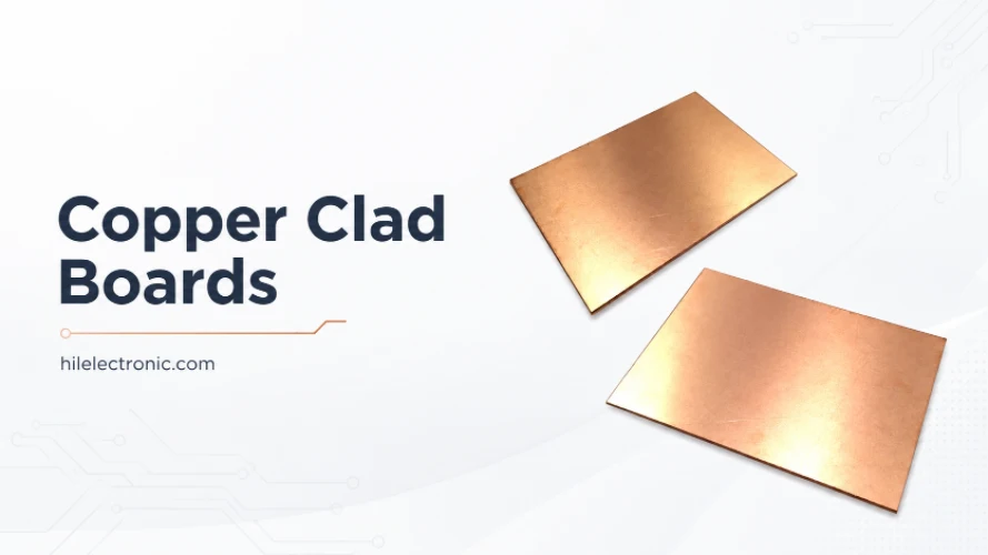
Copper Clad Boards (Copper-Clad Laminate): What They Are, Types, and How PCBs Are Made From Them
Figure 1. copper clad boards image for PCB manufacturing...
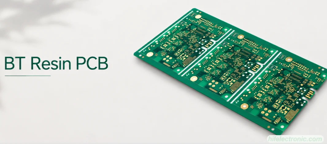
BT Resin PCB: Properties, Uses, and Fabrication Controls
Figure 1. BT resin PCB image for PCB manufacturing...
PCB Potting Services: Compounds, Process, and Design Rules
Figure 1. PCB potting services image for Highleap...
How to get a quote for PCBs
Let us run DFM/DFA analysis for you and get back to you with a report.
You can upload your files securely through our website.
We require the following information in order to give you a quote:
-
- Gerber, ODB++, or .pcb, spec.
- BOM list if you require assembly
- Quantity
- Turn time
In addition to PCB manufacturing, we offer a comprehensive range of electronic services, including PCB design, PCBA (Printed Circuit Board Assembly), and turnkey solutions. Whether you need help with prototyping, design verification, component sourcing, or mass production, we provide end-to-end support to ensure your project’s success. For PCBA services, please provide your BOM (Bill of Materials) and any specific assembly instructions. We also offer DFM/DFA analysis to optimize your designs for manufacturability and assembly, ensuring a smooth production process.