
Back to blog
Introduction to PCB and Different Types of Circuit Boards
PCBs provide the foundation for almost all modern electronics, from simple toys to advanced supercomputers. Serving as the platform for mounting and interconnecting electronic components, the design and materials used in PCBs have a profound impact on the overall function and capabilities of electronic devices.
This comprehensive guide covers the key basics of PCBs first. It then provides details on the most common PCB variants used across consumer and industrial electronics along with the applications, advantages, and tradeoffs of each type.
What is a Printed Circuit Board?
A printed circuit board consists of an insulating substrate material reinforced with layers of conductive copper traces in defined patterns. Electronic components and integrated circuits mount onto the PCB to achieve functionality. The conductive traces interconnect various mounted parts, allowing signals and power to flow. PCBs thus provide the pathways for components to operate together as an electronic system or subassembly.
While early circuit boards were painstakingly hand-wired using point-to-point wiring, the advent of photolithographic fabrication enabled the first true printed circuit boards. By chemically etching copper layers to form traces in almost any intricate pattern, PCBs enabled automated, high-volume manufacturing of sophisticated electronic systems.
Materials used as the foundation PCB substrate include fiberglass composites like FR-4, more advanced thermoset or thermoplastic composites, ceramics, or in some cases, aluminum or steel for applications requiring thermal conduction. The choice of PCB substrate sets fundamental constraints on factors like operating temperatures, dielectric properties, thermal dissipation, and manufacturing processes.
PCBs continue advancing to serve emerging requirements around density, signal speeds, power handling, and reliability through continual developments in materials, interconnect technologies like high-density interconnect (HDI) and blind/buried vias, specialized treatments like immersion gold or ENIG, and fabrication processes attaining finer tolerances and smaller features.
Key Benefits of Using Printed Circuit Boards
While the earliest electrical devices used manual wiring or primitive single or dual-layer boards, multi-layer PCBs now dominate modern electronics due to major benefits including:
- Complexity – Multi-layer boards accommodate extremely intricate circuits with vast numbers of components and dense routing connectivity unachievable by hand.
- Miniaturization – Carefully routed PCBs greatly reduce size and eliminate bulky mechanical connectors between subassemblies. Microvias facilitate further shrinkage.
- Reliability – Automated, high-precision PCB manufacturing results in extremely consistent quality that removes errors inherent in manual wiring.
- Thermal Management – Certain PCB materials provide far better heat conduction and spreading than alternatives as power levels rise in electronics.
- Speed – Tightly controlled trace geometries on PCBs enable precise impedance matching essential for high-speed signals up to multi-GHz frequencies.
- Serviceability – Modular subassembly PCBs simplify diagnostics and field replacement compared to monolithic constructions.
- Scalability – Once initial prototypes are verified, flexible PCB fabrication processes allow extremely rapid scale-up to high-volume production.
- Standardization – Standard form factors, mounting holes, connectors etc. facilitate integration of modules from diverse suppliers across supply chains.
- Testability – Designed-in test points, boundaries, and access supports manufacturability and field diagnostics.
This unique blend of benefits will sustain PCBs as the backbone of electronic systems across consumer gadgets, appliances, automobiles, communication infrastructure, industrial automation, defense systems, and more for the foreseeable future.
Types of Printed Circuit Boards
While all PCBs share common foundations, the enormous diversity of electrical systems dictates a wide spectrum of PCB materials, construction approaches, densities and other characteristics tailored to applications. Here are the most prevalent categories and types of PCBs in use:
1. Single-Sided PCBs
Single-sided PCBs utilize a single thin copper layer laminated onto an insulating phenolic or fiberglass composite substrate. The simple construction makes these the lowest cost PCB option.
Applications: Low complexity circuits including power supplies, analog processing, and lighting
Advantages: Cheapest option; supports high volume production; easy to design and repair
Limitations: Very limited interconnects and component densities
2. Double-Sided PCBs
Double-sided PCBs overcome single-layer interconnect restrictions by adding a second conductive foil layer paired with plated through-holes linking both sides.
Applications: Suitable for moderate complexity circuits like industrial controls, test gear, and LED lighting.
Advantages: Enables greater component densities; more economic than multilayer for less complex systems; facilitates some SMT parts.
Limitations: Still space constrained relative to multilayer; avoids ultra fine pitch ICs.
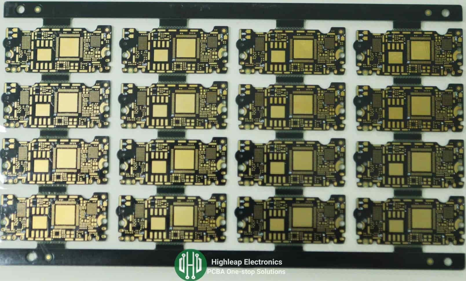
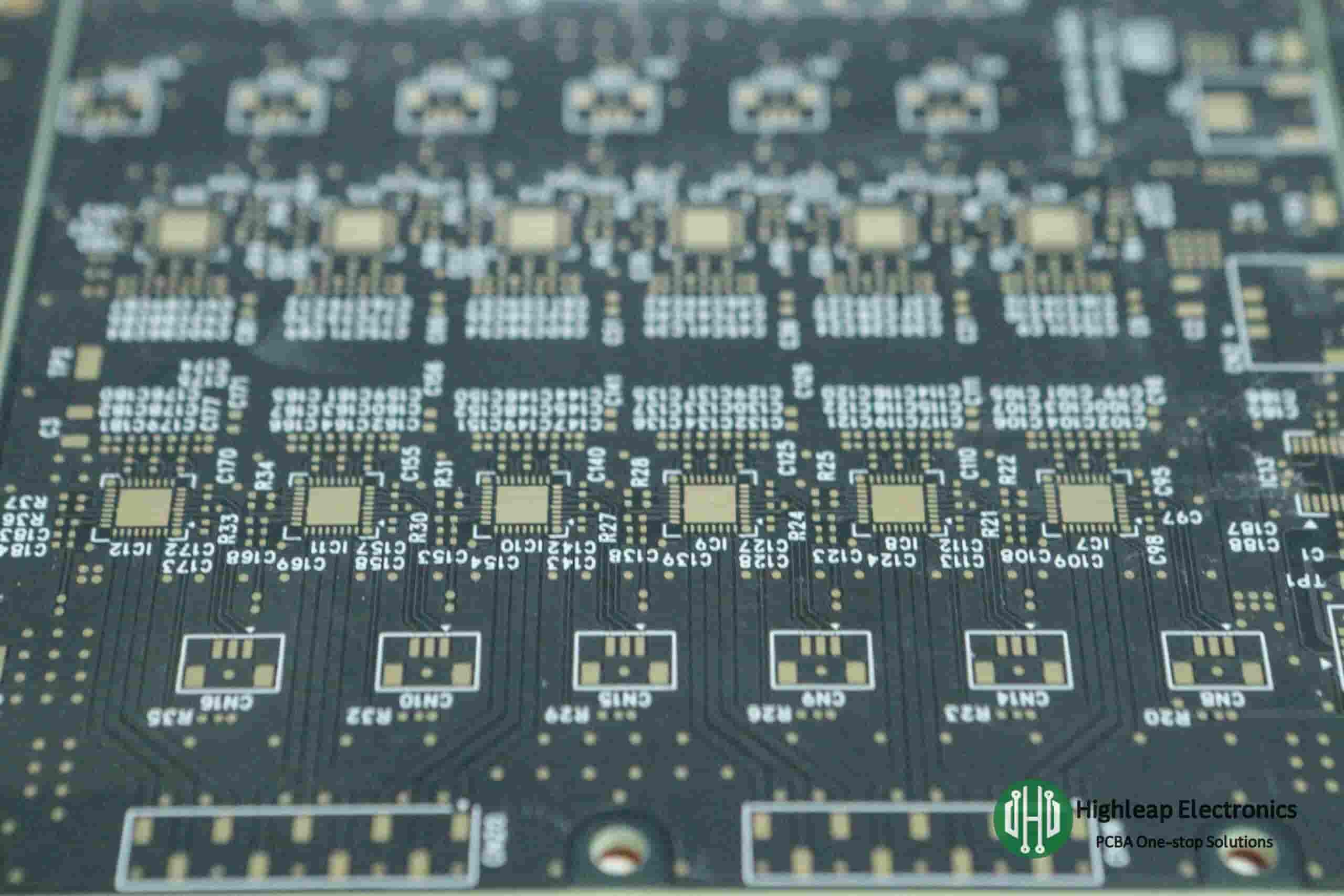
3. Multilayer PCBs
Stacking multiple conductive and insulating dielectric core substrate layers connected by microvias supports extremely dense, complex routing unachievable through other means. These multilayer PCBs dominate advanced electronics like phones, computers, automotive electronics, and medical systems.
Advantages: Enables vastly greater complexity, component density, miniaturization, and functionality integration in compact, affordable packages.
Tradeoffs: Substantially higher fabrication costs and challenging signal/power integrity designs. Difficult manual repair.
4. Flexible PCBs
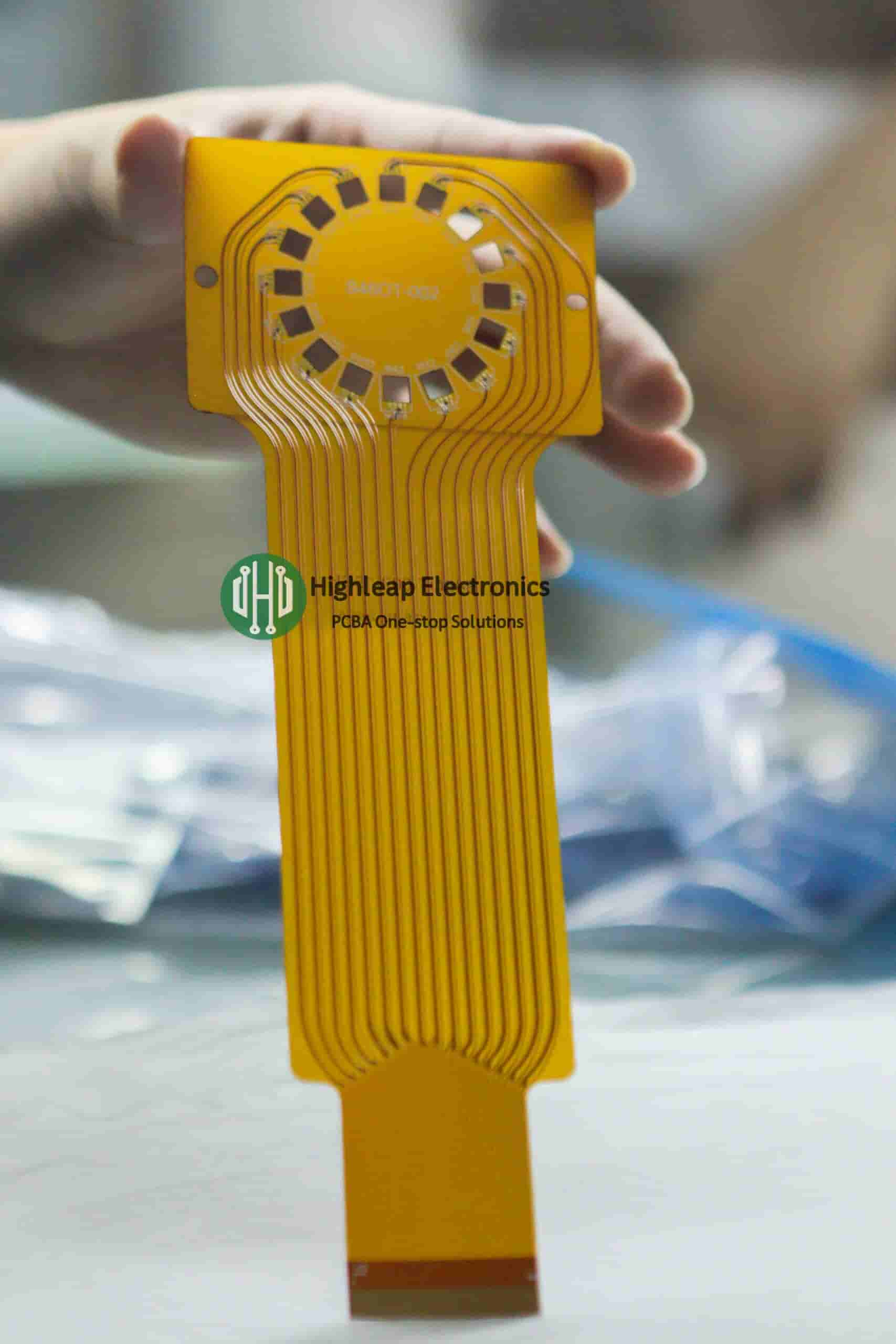
Flexible substrates fabricated from robust polymer films allow bending PCBs to fit irregular contours inside restrictive product enclosures while surviving mechanical stresses.
Applications: Ideal for wearables, medtech devices, military systems where space is extremely constrained.
Advantages: Conforms to complex shapes; lightweight. Withstands flexing, vibration, twisting.
Limitations: Much higher cost; supports only simpler circuits. Requires adhesives.
5. Rigid-Flex PCBs

Combining rigid board areas to mount complex components and routing with thin flex circuit interconnects facilitates extremely efficient 3D layouts inside tight irregular contours.
Advantages: Uniquely blends rigid and flex capabilities enabling space savings and innovations in industrial design.
Considerations: Far higher cost; low/mid-volume niche; very challenging fabrication logistics and design complexity.
6. HDI PCBs
High-density interconnect (HDI) PCBs with microvias, fine lines and spaces, and thin dielectrics support advanced portable devices and high-speed computing packing thousands of interconnects within a square inch.
Advantages: Compact complexity; speed; economical versus low volume, labor-intensive alternatives.
Considerations: Requires significant design expertise, modeling, prototyping to assure good signal integrity, power delivery, and manufacturability.
7. Aluminum PCBs
Replacing conventional insulating substrates with thermally conductive aluminum metal core PCBs transfers heat efficiently from high-power components like LED drivers.
Applications: LED fixtures, automotive converters, power supplies, motor drives
Advantages: Extremely effective heat spreading; handles high power densities. Withstands mechanical abuse. Lower cost than exotic composites.
Limitations: Primarily simple circuits; heavy; corrosion risks without protective measures.
8. LED PCBs
LED PCBs feature thick copper layers to distribute heat combined with low thermal resistance dielectric materials critical for LED luminaries and displays where thermal design strongly impacts cost, reliability, brightness consistency, and lifetime.
Advantages: Excellent thermal dissipation properties to manage heat from high brightness LEDs. Allows smaller LED modules.
Considerations: Material choice, trace widths, hole plugging all tuned for thermal transfer. Often metal core or ceramic substrates.
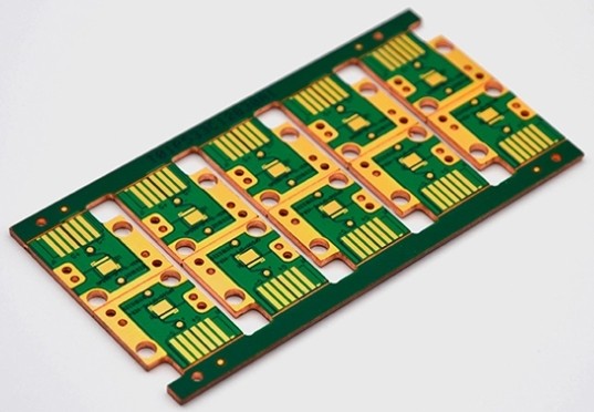
9. FR-4 PCBs
FR-4 fiberglass reinforced epoxy laminate offers an economical balance of capabilities to serve as the default mainstream PCB substrate for the majority of cost-sensitive consumer and light industrial electronic systems not pushing extreme envelopes.
Advantages: Mature fabrication processes; moderate electrical performance; low cost.
Limitations: Temperature range restricted to around 130°C for sustained periods; absorption rate can influence electrical properties. Lossy above a few GHz.
10. High-Frequency PCBs

Communications infrastructure, aerospace avionics, defense electronics and scientific instrumentation demand specialized PCB materials with precisely controlled electrical characteristics to function across microwave, millimeter-wave and multi-gigahertz spectrums.
Benefits: Enables low-loss transmission up to 100GHz; manages dielectric constants and low skew across frequencies bands.
Considerations: Much higher expenses; limited board sizes; challenging modeling and simulations required.
11. High-Temperature PCBs
Automotive electronics, military avionics, geothermal instrumentation and downhole drilling equipment benefit from robust, low-expansion PCB materials able to operate reliably above 260°C for thousands of system lifetime hours as dictated by these long-field-life applications.
Advantages: Operates reliably above 260°C for extended durations; withstands extreme cycles. Low thermal expansion. Materials avoid charring/warping. High rigidity.
Tradeoffs: Extremely costly; very long lead times; repairs unlikely.
12. Metal Core PCBs

Selecting a metal substrate like aluminum or copper versus conventional insulating laminates forms a heat spreader allowing metal core PCBs to dissipate intense heat loads from high-power components common in electric vehicle traction inverters, server CPUs, RF amplifiers, power supplies and similar applications.
Advantages: Extremely high thermal conductivity efficiently transfers heat from hot components to ambient air. Handles high continuous power densities. Withstands mechanical abuses.
Limitations: Primarily deployed in cost-sensitive simple circuits with minimal routing; heavier than composites; risks galvanic corrosion.
13. Thick Copper PCBs
Doubling or quadrupling conventional 1-2 ounce copper foil thickness to 4 or 8 ounces serves applications like data processing servers and telecom hardware packing many high speed signals in parallel transmission line configurations benefitting from lower losses and crosstalk achieved using the thicker traces.
Benefits: Lower loss at high frequencies or DC current densities improves performance; thicker conductors facilitate heavier plating if needed.
Tradeoffs: Much longer fabrication times and lower yields increase expenses substantially; only applicable to simplistic multi-signal layer routings.
This framework of the 13 predominant PCB variants applied across diverse electronics sectors helps tailor selections to optimize technical design objectives, operating environs, product lifetimes and costs.
Conclusion
Printed circuit boards establish the foundation for interconnecting and operating all electronic components and ICs to achieve system-level functionality. The continual evolution of PCB materials, fabrication capabilities, signalling techniques, thermal management and packaging drives exponential expansions in processing speeds, data bandwidths, embedded intelligence and nearly every figure of merit around electronics.
Understanding the spectrum of PCB technologies available along with their respective strengths and weaknesses assists design engineers in navigating tradeoffs around cost, capabilities and physical constraints

Recommended Posts

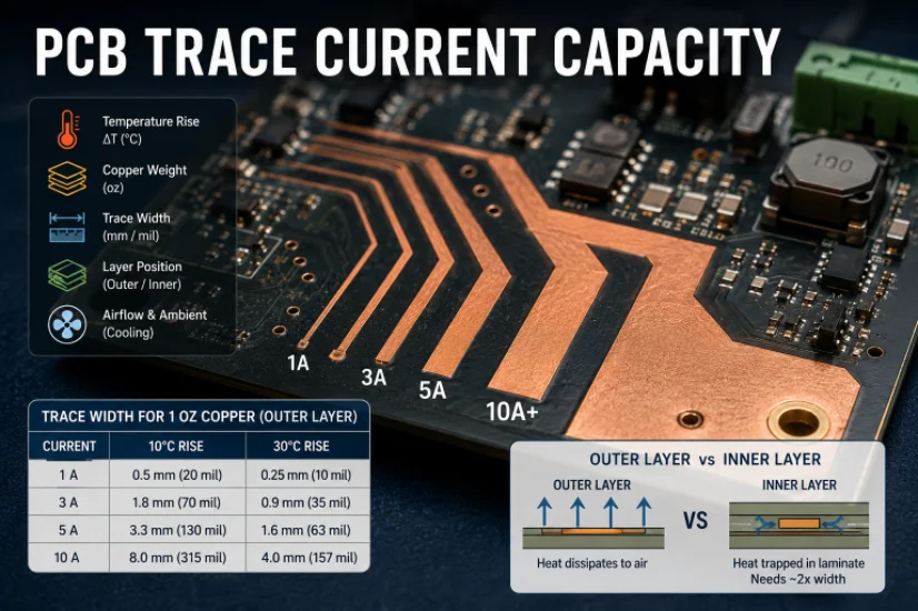
PCB Current Calculator: Sizing Trace Width and Vias with the IPC-2221 Formula
Figure 1. Pcb Current Calculator reference image for PCB...
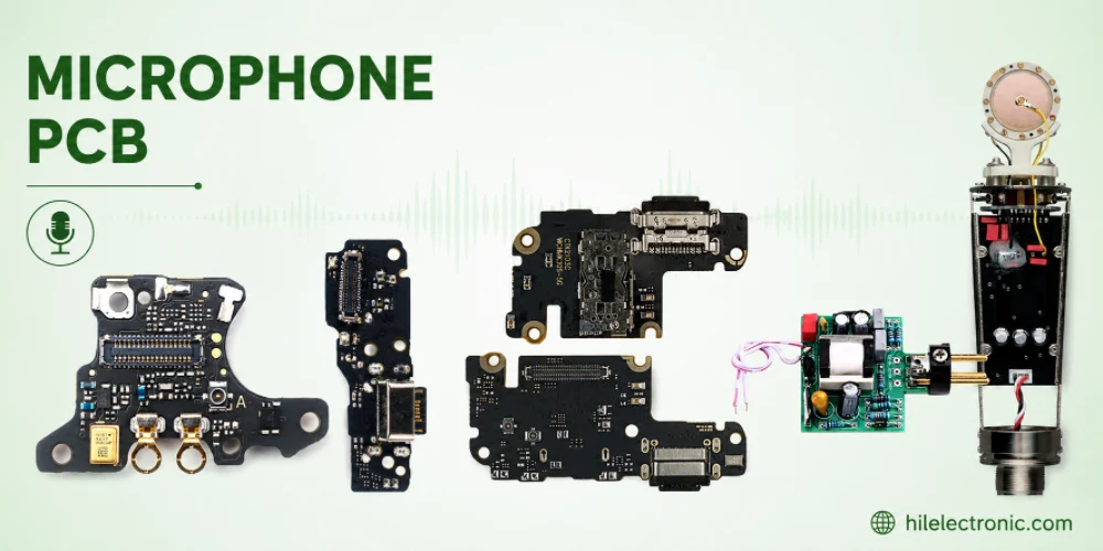
Microphone PCB Design: How the Board Itself Shapes Your Audio Quality
Figure 1. Microphone Pcb reference image for PCB...
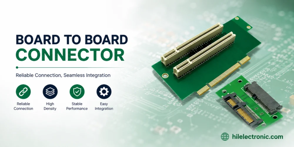
Board-to-Board Connector: Types, Specifications, and How to Select One
Figure 1. Board To Board Connector reference image for PCB...
PCB Trace Width Calculator: How to Size Traces for Current, Voltage Drop, and Impedance
Figure 1. A PCB trace width calculator is a starting point...