
Back to blog
PCB Design: 5 Mistakes Need To Be Avoided

The cost implications of errors made during the PCB design phase can be substantial, affecting not only the financial aspects but also the timeline and overall success of a project. To mitigate these risks and ensure that PCBs meet industry standards, designers need to adopt a proactive approach that emphasizes accuracy, compliance, and foresight. Here are five common PCB design mistakes that need to be avoided:
Ignoring Design for Manufacturability (DFM) Guidelines
Design for Manufacturability (DFM) checks should be conducted early and throughout the design process. These checks help identify potential manufacturing issues before they become costly errors. DFM guidelines cover aspects like trace widths, spacing, via sizes, and pad dimensions, ensuring the PCB can be manufactured reliably and efficiently.
- Trace Widths and Spacing: Ensuring that trace widths are appropriate for the current they will carry and that spacing meets minimum requirements to prevent short circuits and ensure electrical isolation.
- Via Sizes and Pad Design: Designing vias and pads to be of sufficient size for the manufacturing process, including considerations for aspect ratio (drill size to board thickness) and ensuring pads are large enough to support component leads without risking detachment.
- Component Placement and Orientation: Placing components in a manner that supports efficient and reliable soldering, taking into account thermal management, and minimizing the risk of assembly errors.
- Panelization and Board Edge Requirements: Designing PCBs to fit within standard panel sizes and including necessary features for handling and processing during manufacturing, such as breakaway tabs and tooling holes.
- Material Selection: Choosing materials that are compatible with the intended manufacturing processes and final application environment, considering factors such as thermal expansion, moisture absorption, and dielectric properties.
- Annular Rings and Drill Tolerances: Ensuring that annular rings around vias are of sufficient size to account for drill tolerances, reducing the risk of breakout and ensuring reliable electrical connections.
- Layer Stackup and Impedance Control: Designing the PCB layer stackup to achieve the desired impedance characteristics for high-speed signals, which involves careful selection of materials and control of trace geometry.
For a more complete production review, use this article alongside rigid-flex circuit production and metal core PCB manufacturing when checking stackup, assembly, or test requirements.
Poor Power and Ground Plane Management
Power integrity and signal integrity are critical for the proper functioning of the PCB. Poor management of power and ground planes can lead to issues like noise, interference, and inadequate power supply to components. It’s important to ensure that power and ground planes are properly distributed, and decoupling capacitors are used appropriately to stabilize power supply.
- Use Decoupling Capacitors: Decoupling capacitors should be placed close to the power pins of integrated circuits to stabilize the local power supply and filter out high-frequency noise.
- Plan for Thermal Management: Incorporate thermal vias and consider the placement of high-power components to ensure effective heat dissipation across the PCB.
- Ensure Proper Layer Stacking: A well-thought-out layer stack-up can significantly improve power integrity and signal integrity. Placing power and ground planes close to each other can reduce loop area and minimize EMI.
- Minimize Ground Loops: Design the layout to minimize ground loops, which can introduce noise into the system. This includes careful routing of ground connections to prevent large loop areas.
- Use Multiple Power and Ground Planes: For complex boards with multiple voltage levels and high-current paths, using multiple dedicated power and ground planes can help in distributing power more evenly and isolating sensitive circuits from noise.
- Implement Proper Plane Partitioning: Partitioning power planes according to different circuit sections (e.g., analog and digital) can help reduce interference between them. It’s crucial to maintain solid ground planes whenever possible to avoid creating discontinuities that can act as radiating elements.
- Maintain Low Impedance Paths: Ensure that the impedance between the power source and the load is minimized to prevent voltage drops and ensure stable power delivery.
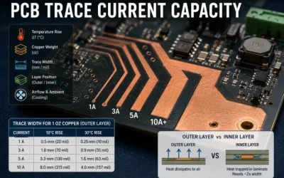
Inadequate Spacing and Trace Widths
Traces that are too narrow can increase the resistance of the circuit, leading to voltage drops and overheating. Conversely, traces that are too wide can take up unnecessary space and complicate the routing of other signals. Similarly, inadequate spacing between traces can lead to short-circuiting and cross-talk. Ensuring that trace widths and spacing meet the requirements for the expected current loads and signal integrity is crucial.
- Short Circuits: Insufficient spacing between traces can lead to short circuits, either during the manufacturing process due to etching errors or later due to material expansion, contraction, or debris causing a bridge between traces.
- Electrical Interference (Crosstalk): Traces that are too close to each other can induce electrical interference in adjacent traces, known as crosstalk. This can degrade signal integrity, especially in high-speed circuits.
- Increased Heat and Potential for Trace Failure: Trace widths that are too narrow for the current they carry can overheat, potentially causing the trace to fail. This can result in open circuits or, in severe cases, damage to the board or components.
- Impedance Mismatch: In high-speed or RF circuits, trace width is critical for controlling impedance. Incorrect trace widths can lead to impedance mismatches, resulting in signal reflections, attenuation, and loss of data integrity.
- Manufacturability Issues: Inadequate spacing can lead to difficulties in the manufacturing process, including problems with solder mask application, etching, and achieving reliable solder joints. This can increase the defect rate and production costs.
Not Accounting for Thermal Management
Electronic components generate heat, and without proper thermal management, this heat can build up, leading to component failure. It’s important to consider heat dissipation in the design, which might include the use of heat sinks, thermal vias, and the strategic placement of components to improve airflow.
- Use Thermal Vias: Thermal vias can help transfer heat from the top layers of the board to the bottom layers or to a heat sink. They are particularly useful for high-power components or areas with high thermal loads.
- Implement Heat Sinks and Heat Spreaders: Heat sinks can be attached directly to heat-generating components to dissipate heat into the surrounding air. Heat spreaders can be used to distribute heat more evenly across the board.
- Optimize Component Placement: Place heat-generating components in a way that allows for efficient heat dissipation. Avoid clustering high-power components together to prevent the creation of hot spots.
- Use Heavy Copper Traces for Power Layers: Heavier copper traces have lower resistance and are more effective at conducting heat away from components. This can be particularly useful for power distribution layers.
- Incorporate Thermal Relief Pads: Thermal relief pads can be used to reduce the heat transferred from a component to the PCB, helping to protect sensitive components from overheating.
- Consider Board Material: The choice of PCB material can affect thermal conductivity. Materials with higher thermal conductivity can help spread heat more efficiently, reducing hot spots.
- Optimize Airflow: Design the PCB layout and enclosure to optimize airflow. Proper ventilation can significantly improve heat dissipation through natural or forced convection.
- Simulation and Thermal Analysis: Use simulation tools to perform thermal analysis during the design phase. This can help identify potential thermal issues before the board is manufactured, allowing for design adjustments.
- Use Multilayer Boards: Multilayer boards can provide additional layers for heat dissipation. Power and ground planes, in particular, can act as heat spreaders.
Overlooking Signal Integrity
High-speed signals are susceptible to various forms of distortion, such as reflection, crosstalk, and attenuation. Failing to account for signal integrity can lead to unreliable or non-functional circuits. Designers need to consider the routing of high-speed signals carefully, use differential pairs when appropriate, and minimize the length of critical signal paths.

Related Articles
PCB Trace Width Calculator: How to Size Traces for Current, Voltage Drop, and Impedance
Size PCB trace width for current, voltage drop, internal and external layers, controlled impedance, and fabrication tolerance.

Protel PCB: Is It the Same as Altium Designer, and How to Open Legacy Protel Files
Open legacy Protel PCB files, migrate designs into Altium, check old libraries and nets, and export clean PCB manufacturing data.

PCB Trace Resistance Calculator: How to Calculate Trace Resistance and Voltage Drop
Calculate PCB trace resistance, voltage drop, power loss, and copper width choices for reliable fabrication and power delivery.