
Back to blog
Common PCB Failure Modes and How We Avoid Them
PCBs have become indispensable foundations across consumer and industrial electronics. However, these complex, multi-technology modules also invite defects stemming from intricate fabrication processes, challenging component assembly techniques, harsh operating environments, and simple wear over time.Common electronic component failures include mechanical, thermal, environmental, electrical stress, packaging, and aging.
Without diligent quality control and process validations, latent flaws or excessive deterioration can swiftly transform an innocuous manufacturing anomaly into a catastrophic field failure mechanism resulting in dreaded customer returns, expensive warranty expenses, tarnished reputations, and lost sales.
This comprehensive guide examines the most prevalent PCB failure modes, defect origins, inspection methods, remedial actions, and mitigation strategies to arm engineering and operations teams with the awareness needed to uphold product reliability.
The Scale of PCB Usage and Associated Failure Risks
Printed circuit boards reside at the core of nearly every electronic device. Demand has skyrocketed in recent years, with global PCB sales expanding over $3.7 billion annually since 2010 to surpass $75 billion as of 2021 according to industry association data.
This tremendous scale translates into billions of PCBs across an immense diversity of applications experiencing continuous stress under a myriad of voltage, power, temperature, vibration and other environmental conditions plus inevitable material aging. Even extraordinarily minuscule defect rates still accumulate substantial failure volumes.
By delving into common failure origins, sensible prevention policies, pragmatic inspection approaches, and efficient rework processes, manufacturers achieve heightened quality levels that reduce expenses while protecting end customer experiences.
PCB Failure Definition, Impact, and Diagnosis Challenges
A failed printed circuit board no longer executes its intended functions adequately due to either catastrophic electrical shorts, opens, or out-of-tolerance performance relative to original specifications. Intermittent failures represent an especially vexing category to troubleshoot.
The failure mechanism and root cause may reside in the PCB itself or attachments like connectors, wire bonds, and solder joints. Regardless, the operational and economic impacts rapidly compound as the failed board probably constitutes an essential subsystem within a larger product also consequently impaired.
Unlike discrete semiconductor component failures plainly localizable using basic diagnostic equipment, intricate PCB construction complicated by miniaturized, multi-layer SMD circuit packs impedes easy fault isolation without X-ray tools. This hindrance demands upfront design forethought enabling testability.
Critical PCB Failure Categories with Origins and Prevention Strategies
Plating Voids
Spotty metal deposition inside plated through-holes brings susceptibility to opens under thermal or vibration stresses as substandard continuity and adhesion provoke fractures. Prevention centers on contamination controls, proper catalyst activation, uniform copper distributions, and smoothed hole walls.
Insufficient Edge Clearances
Too little spacing between copper traces and board peripheries risks shorts from condensation or handling damage given the thinness of typical protective coatings. Conservative spacing rules plus thorough DFM analysis prevents such lapses.
Cold Solder & Other Joint Defects
Incomplete reflow, chronic movement, contamination, or long-term material migrations jeopardize interconnections critical for power transmission and signaling integrity. Process validations, materials improvements, training, and inspection checklists bolster assembly quality.
Etching-Related Copper Slivers
Redeposited metal fragments bridge unrelated conductors or penetrate coatings to enable eventual short circuits from applied condensation or voltages exceeding insulation thresholds. Tight pattern density controls accompanied by more aggressive wash cycles reduces defect rates.
Exposed Inter-Pad Copper
Age, abrasion, or simply inadequate solder masking during fabrication removes vital insulation layers separating adjacent metallic surface-mount landing pads vulnerable to shorting from environmental moisture or electrical arcing. Conservative mask dam widths plus improved mask properties helps.
Other Common PCB Risk Factors
- Acute etching agent entrapments
- Electromagnetic interference
- Substandard components
- Thermal strains across interfaces
- Material impurities & dendrites
By spotlighting the predominant PCB failure mechanisms frequently accelerating infant mortality rates and abruptly ending operational lifetimes, engineers can prioritize mitigation initiatives targeting those weaknesses with the most severe repercussions.
Employing Inspection Methods for Early PCB Defect Detection
Since each manufactured board expends significant material and labor costs, rapidly detecting both visible assembly defects and hidden latent damage from disturbed process control aids productivity by either correcting or scrapping bad boards earlier while also providing feedback to improve statistical yields.
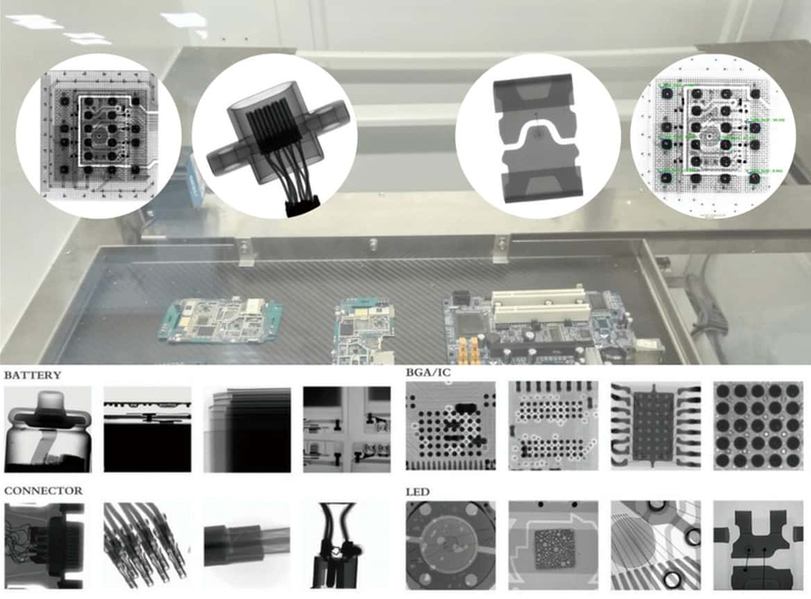
X-ray imaging stands apart as the most valuable inspection technique given penetration beyond easily accessible outer surfaces to reveal underlying conditions. Lacking such fantastical vision, engineers employ a diverse assortment of pragmatic approaches:
Visual Audits – Bright lighting, magnification, and pattern familiarity facilitates identifying missing or misaligned components, scratch damages, discoloration, inconsistent joints and board warpage.
X-Ray Inspection – Closed internal solder voids, cracks, contamination, separation of material layers, and hidden fractures appear opaque under X-ray examination relative to properly bonded surrounding materials.
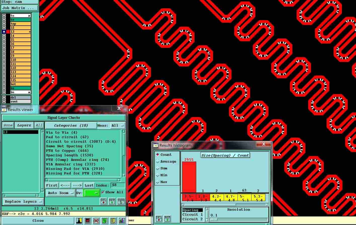
Optical Inspection – High resolution cameras digitally map board artwork geometries, component placements, and textual serial numbers to automatically flag deviations from computer aided manufacturing (CAM) data through pattern matching algorithms under challenging production tempos.
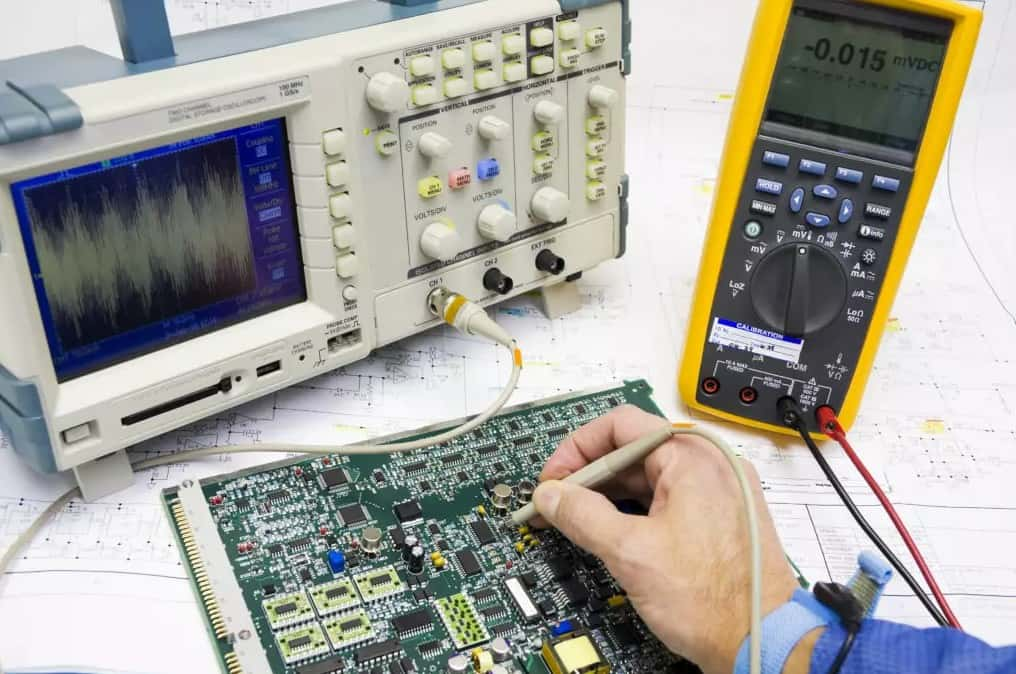
Electrical Testing – Rather than inspecting physical constructions, in-circuit testing probes electrically exercise interconnected nets with dynamic signal inputs while monitoring functional outputs and parametric performance metrics like currents, voltages, frequencies, and modulation patterns for conformance to specifications.
By deploying the right inspection recipe matching cost and capabilities to value and vulnerability for a particular product, manufacturers sustain consistent quality standards.
Overview of Corrective Measures Responding to PCB Deficiencies
No amount of designing, processing or inspection vigilance elicits perfect production yields devoid of occasional deficiencies escaping detection to the field. Resolving issues efficiently preserves operational continuity.
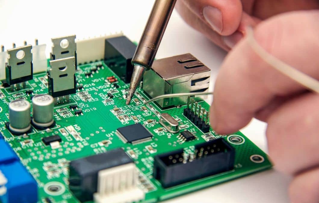
Rework – Skilled technicians utilize specialized micro-soldering irons, heaters and other intricate tools to remove defective components and re-populate boards with replacements restored to functional status after extensive testing.
Troubleshooting – Rather than immediately discarding, deeper fault isolation techniques involving voltage injections, thermal imaging and electrical signatures characterize failure origins and mechanisms to indicate potential wider process adjustments improving entire populations.
Design Revisions – For recurring issues traced to marginal or sensitivity circuit architectures, board revisions add adjust component values, trace widths, layer stackups, and performance guardbands to strengthen robustness.
Process Tuning – Shifting environmental parameters like temperature set points, transport speed,lamination pressure, or chemistries alter fabrication outputs to curtail defect precursors.
Supplier Engagements – Collaborative root cause investigations incorporating substrate experts, chemical formulators, assembly specialists, and equipment technicians brings multifaceted perspectives exposing nuanced improvement opportunities.
Repairs – In scenarios where rework lags practical, some larger modules permit targeted repairs, contractions, or augmentations restoring asset functionality faster and cheaper than total replacements if degradation stays localized.
By deploying the optimal restoration pathway specific to defect profiles, likelihoods, and downstream risks, manufacturers sustain factory and field return metrics exceeding six sigma quality level benchmarks demonstrating continuous advancement rather than stagnation.
Conclusion
Defect-free, failure-immune printed circuit boards matching exponentially expanding electronics functionality demands while paralleling plunging consumer prices remain elusive despite herculean efforts specification precisions, quality certifications, and process penalties slashing parts per million defect rates to hitherto unfathomable single digit levels.
Economic realities compel accepting some fractional failure incidence through astute risk balancing rather than chasing absolute perfection with negligible practical gains at disproportionate costs. Instead, sensible prevention policies targeting known vulnerabilities governed by high severity and likelihood, coupled with rapid containment protocols circumscribing damages through responsiveness, best serve to maximize productivity and reliability.

Recommended Posts
What is a Cold Joint Solder and How Can You Prevent it?
[pac_divi_table_of_contents title="On this article"...

Demystifying BGA Soldering: Tips and Best Practices
[pac_divi_table_of_contents title="On this article"...

Selecting the Right PTFE Material for Your PCB
[pac_divi_table_of_contents title="On this article"...

20 Analog Circuits Engineers Should Master
[pac_divi_table_of_contents title="On this article"...